Simulated and experimental conclusions of temperature imbalances show significantly more efficient cooling around the outside of corners.
Through the years, the impact of right-angle corners on printed circuit board (PCB) traces has been a hot topic. As early as the 1990s, some were arguing strongly against the use of 90˚ corners, using mitered corners instead. They based this recommendation, typically, on one of two reasons:
- The width of a typical PCB trace increases as the trace turns a corner. This increases the local capacitance at that point, lowering the trace impedance. This impedance discontinuity can therefore set up a reflection that can lead to signal integrity issues.
- The current density around a trace corner shifts so that it is strongest at the inside edge of the corner, where the path length is the shortest. This increased current density can lead to an increase of the local electromagnetic field, which can subsequently lead to increased EMI from the trace.
In a landmark paper published in 19981, Brooks tried to put these arguments to rest. In that paper he showed:
- Although it is true the width increases, it does not increase much. Further, the maximum width occurs at a point, not over a range. And finally, the entire signal path around the corner is much shorter than the “critical length2.” Therefore the impedance discontinuity is insignificant.
- An empirical investigation of actual EMI measured from traces with various corner designs, including a diabolical 135° corner with sharp “points” — which would never be found on a PCB! — showed no significant radiation greater than a control “straight” trace.3
A more recent paper4 shows an image of a 10mm (400 mil) wide, 35µm (1.0oz.) trace thickness, heated to approximately 80˚C. The image suggests there is about a 3˚C difference between the outer edge of the trace and the inside corner. The authors conclude:
This corner effect decreases the CCC (current carrying capacity) of bended traces compared to straight trace with the same width ….Value will be added if CCC design chart for bended traces can be a part of future PCB trace thermal design guideline.
This paper looks at the thermal gradients around the corners on a PCB.
Trace Heating and Cooling Dynamics
PCB traces heat by I2R power dissipation in the trace. Traces cool by conduction through the board material, convection through the air, and by radiation. Temperature stability occurs when the rate of heating equals the rate of cooling.
Conduction through the board material is the predominant cooling mechanism on a typical PCB. Conductive cooling occurs in two directions: “in-plane” (parallel to the traces) and “through-plane” (through the board perpendicular to the traces). “In-plane” conduction is the predominant mechanism of the two.
Brooks and Adam have demonstrated a thermal gradient across the trace, hottest along the centerline and cooling out toward the edge of the trace.5 This is because of “in-plane” conduction and the fact that the cooling path is shorter for heating at the edge of the trace than it is at the centerline of the trace. This fact will be important in the discussion below.
Software Simulation
We used a thermal simulation software tool (TRM6) to look at traces with right-angle corners. Four corner configurations were looked at, as illustrated in FIGURE 1.
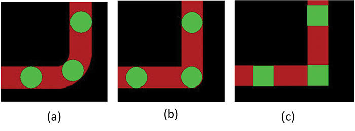
Figure 1. Four different corner configurations.
Configuration A is a constant width corner; i.e., the trace is the same width everywhere. It has a rounded inner corner. Configuration B is typical of a trace found on a PCB. It is typically created by “drawing” a trace with a circle (whose diameter is the same as the trace width). Configuration C is a “square” corner, rarely seen on a PCB, and actually somewhat difficult to create on a PCB. (It can be drawn with a square aperture on some plotters.) It should be noted the width across the corner, and therefore the trace cross-sectional area at the corner, is the same as the body of the trace for configuration A, but increases as we move to configurations B and then C.
The basic model used was a 5mm (200 mil) wide, 35µm (1.0 oz.) trace on a standard 1.5mm-thick FR-4 substrate. Two trace configurations were modeled: configuration A, a rounded, constant width corner, and configuration B, typical of what would be “drawn” with a Gerber file with a 5.0mm round aperture. A current of 8.0A was modeled, resulting in a temperature of approximate 44˚C (about a 24˚C increase.) A TRM model allows us to investigate (among other things) both the current density and the thermal characteristics around the corner.
FIGURE 2 shows the current density (A/mm2) around the corners of the traces. The shift in current from the outside corner to the inside corner is fairly dramatic, especially for configuration B, where the inside corner is sharp7. This is directly related to the path length of the current around the corner, that path being significantly shorter along the inside edge.

Figure 2. Current density around the corners of 5.0mm, 35µm (1.0 oz.) traces carrying 8.0A.
One might speculate the increased current density at the inside edge of the corner would lead to a temperature increase along the trace at that spot. Another argument, however, might be the thermal conductivity of the copper is so high no temperature gradients could develop. FIGURE 3 shows thermal profiles for the two configurations modeled. The small boxes record the temperature at the upper left corner of the box.
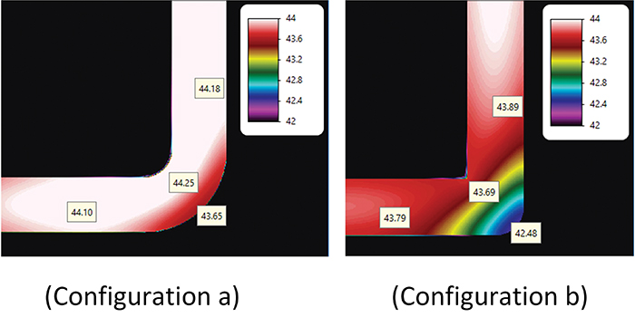
Figure 3. Thermal profile around the corners of the modeled traces. The temperature range shown is between about 42˚ and 44˚C.
The model suggests the trace temperature is slightly warmer at the inside edge of configuration (A) than at the outside edge. The inside edge is about 1.3° warmer than the outside edge of the sharper configuration (B).
But it turns out the heating dynamics around the corners are much more complex than this. FIGURE 4 illustrates the thermal profiles of the traces and of the board around the traces. Note the board around the inside of the corners has a wider thermal profile than around the outside of the corner. This indicates the outside of the corner is cooling more efficiently than the inside of the corner. At least four factors contribute to the thermal profile of the trace and the surrounding area:
- If the cross-sectional area of the corner is larger than the cross-sectional area of the rest of the trace, the “point” resistance around the corner will be lower than the “point” resistance along the rest of the trace. Therefore, the temperatures around the corner will tend to be smaller than along the rest of the trace.
- The current density is significantly higher toward the inside of the corner than toward the outside of the corner. Therefore, the “point” I2R power dissipation will be higher at the inside of the corner than at the outside of the corner.
- The thermal conductivity of the copper trace is so high that some heat generated at the inside corner will conduct away through the copper to the outside corner.
- Notice how the board area at the inside of the corner tends to be much warmer than at the outside of the corner. This is because the heat from both legs of the trace conducts into the same 90˚ arc of the board on the inside of the corner, but the heat tends to fan out (in a 270˚ arc) away from the outside of the corner. Thus, the outside of the corner cools more effectively than does the inside of the corner. It is likely this is the most important determinant of the trace temperature around the corner.
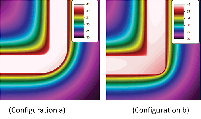
Figure 4. Thermal profile of the modeled traces and the board area around the traces.
Looking back at Figure 3, configuration B, it is true the inside of the corner is warmer than the outside of the corner; it is also true the inside edge is cooler than the midpoint of the straight section of the trace on either end of the corner. This illustrates the impact of the complex relationships outlined in A through D above.
Additional modeling, not reported here, results in the following observations:
- The greater the distance from the inside corner to the outside edge of the curve, the more pronounced the difference in temperature.
- The sharper the inside corner, the more pronounced the difference in temperature. (That is, smooth inside curves result in lower temperature differences around the corner.)
- Narrower traces and/or lower currents result in smaller temperature differences around the corner.
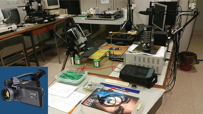
Figure 5. FLIR SC640 IR camera used for investigation (lower left corner) and overview of the experimental setup.
Experimental Investigation
The experimental investigation was performed with a FLIR SC640 infrared (IR) camera with the following specifications: IR resolution (microbolometer grid size) – 640 x 480 pixels, IR spectral range – 7.5 – 13µm (long wave IR), focus – automatic or manual and Focal Plane Array (FPA) based on uncooled microbolometers, which are produced as heat sensors with active layers of vanadium oxide or amorphous silicon placed on a silicon substrate. The electromagnetic radiation in the 7.5 – 13µm range hits the active layer and changes its electrical resistance. This resistance change is measured, processed and transformed by the IR camera into a temperature array, which can be represented graphically by the color display with the IR resolution specified above.
Additionally, for obtaining a better zoom of the thermograms, the authors used a close-up lens 0.5X (over the classical 24° lens, which has a close focus limit of 0.4m), having a focal length of 76.3mm and reducing the close focus limit to 60.3mm.
The test board was designed using Cadence/OrCad 16.6-2015 software and produced in the UPB-CETTI labs using PnP prototyping technology (FIGURE 6).

Figure 6. a. The virtual test board (a) and actual test board (b).
The PCB laminate is a standard FR-4 substrate of 1.5mm with a copper thickness of 35µm. The layout consists of two areas of PCB structures, placed in the upper and lower areas of the board, with the horizontal symmetry line in the middle. The lower area is identical, but mirrored vertically with the upper area. Each area is composed of:
- On the left: one PCB trace of 5mm in width (round aperture) with longer miter, one PCB trace of 5mm in width (round aperture), with shorter miter, and one PCB trace of 5mm in width (round aperture), with fillet/round corner;
- On the right: one PCB trace of 0.5mm in width (round aperture) with right-angle corner (90°), one PCB trace of 2.5mm in width (round aperture) with right-angle corner, one PCB trace of 5mm in width (round aperture) with right-angle corner, and one PCB trace of 5mm in width (square aperture, see Figure 1d) with right-angle corner.
FIGURE 7 presents the IR thermal investigation in progress. The color display of the IR camera shows a real thermal pattern for a 5mm PCB trace (round aperture) with right-angle corner, carrying a DC current of 8.0A, the setup consisting in a high current DC power supply, the test board, and a DMM for measuring ambient temperature, RH and various temperatures based on a K-type thermocouple. The DMM was also used for measuring exactly the DC current injected in the PCB trace.
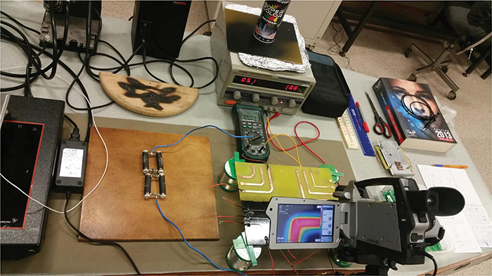
Figure 7. IR thermal investigation in progress.
Codreanu has performed an investigation on the 2.5mm PCB trace (round aperture) with right-angle corner, carrying a DC current of 8.0A, the thermal pattern depicted in FIGURE 8. The temperature distribution (thermal pattern/map) is highlighted and numerically shown by the temperature scale from the right of the picture and the spots on the trace.

Figure 8. Thermogram of the 2.5mm PCB trace (round aperture) with right-angle corner, for 8.0A.
After this, the main focus was to measure all the 5mm PCB configurations (PCB trace (round aperture) with 90° corner, PCB trace (square aperture) with 90˚ corner, PCB trace (round aperture) with shorter miter, and PCB trace (round aperture) with fillet/round corner). FIGURE 9 presents the thermograms of the 5mm PCB trace (round aperture) with 90° corner (left) and of the 5mm PCB trace (square aperture) with 90° corner (right), for a DC current of 8.0A.

Figure 9. Thermograms of the 5mm PCB trace (round aperture) with right-angle corner (left) and of the 5mm PCB trace (square aperture) with 90° corner (right), for 8A.
It was convenient to also record thermograms for a mitered and gently rounded corner. Thermograms in FIGURE 10 show the temperature distribution in the case of the 5mm PCB trace with round aperture, with shorter miter (left, see Figure 6) and with fillet/round corner (right) for a DC current of 8.0A. These results are consistent with the results predicted at the end of the Software Simulation section above.
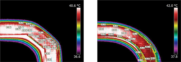
Figure 10. Temperature distribution in the case of the 5mm PCB trace with round aperture, with shorter miter (left, see Figure 6) and with fillet/round corner (right), for 8A.
Conclusions
Current densities around corners are higher at the inside of the corner compared to the outside of the corner. This is consistent with previous studies.
Temperatures are higher at the inside of a corner than they are at the outside of a corner. And there is a close correlation between the modeled data and the experimental data. But these temperatures are not necessarily higher than they are along the main body of the trace. This is because the traces are usually wider at the corner than they are along the main body, and the electrical resistance is therefore lower. Consequently, the I2R heating is lower at that point.
The temperature imbalances around a corner are not likely the result of the difference in current densities. More likely they are the result of the significantly more efficient cooling mechanism around the outside of the corners, where the open board area is much wider.
Notes
1. Douglas G. Brooks, “90 Degree Corners: The Final Turn,” Printed Circuit Design, January 1998, available at ultracad.com.
2. For a discussion of critical length, see Douglas Brooks, PCB Currents: How They Flow, How They React, Prentice Hall, 2013, p. 216.
3. While it is true there are no problems with using right-angle corners on traces, many designers still prefer mitered corners for aesthetic reasons. Some fabricators prefer mitered corners to right-angle corners for fabrication reasons.
4. Yi Wang, S. W. H. DeHaan and J. A. Ferreira, “Thermal Design Guideline of PCB Traces under DC and AC Current,” Energy Conversion Congress and Exposition, September 2009.
5. Douglas Brooks and Johannes Adam, PCB Traces and Via Currents and Temperatures: The Complete Analysis. See Chap. 4 for a full discussion of trace heating and cooling dynamics. See Sect. 12.1 for a discussion of why traces are cooler at the edge than down the centerline.
6. TRM (Thermal Risk Management) was created by Dr. Johannes Adam. TRM was conceived and designed to analyze temperatures across a circuit board, taking into consideration the complete trace layout with optional Joule heating, as well as various components and their own contributions to heat generation. A description of how to construct a basic TRM model can be found in Brooks and Adam, PCB Trace and Via Currents and Temperatures; The Complete Analysis, Chap. 6.
7. If a model has a sharp 90° corner, the mathematics may result in an infinite current density at that specific (infinitely small) point because of a singularity (think divide by zero). This does not have any effect on the rest of the model.
Douglas Brooks, Ph.D. is president of UltraCAD Design (ultracad.com). Norocel Codreanu, Ph.D., is full professor at Politehnica University of Bucharest (UPB), Romania, faculty of Electronics, Telecommunications and Information Technology, and currently executive manager of the UPB university Center for Technological Electronics and Interconnection Techniques (UPB-CETTI). Dr. Johannes Adam, CID, is founder of ADAM Research, a technical consultant for electronics companies, a software developer, and author of the Thermal Risk Management simulation program.