A new alternative using QFNs with open thermal via-in-pad (VIP) structures reduces cost and eliminates solder wicking.
BTC packages were first offered more than 10 years ago. Since then, use has grown steadily, with a significant increase in demand observed over the past three years. BTCs are most commonly offered as QFNs (FIGURE 1). With many benefits and successful market penetration, most packaging houses now provide QFNs, albeit using different names depending on final package format, including MLF, MLPD, MLPM, MLPQ, VQFN, and DFN.
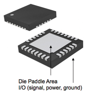
Figure 1. Standard QFN device bottom view.
QFN packages are used to meet a variety of voltage/power regulation, logic controller, and clocking needs. The small form factor is attractive to designers looking to increase functionality using less PCB real estate. A good example is shown in FIGURE 2. Many voltage regulator designs have migrated from using a daughtercard sub-component soldered to the PCB to performing regulation directly on the main card assembly with the use of a QFN, also known as down-regulation or “down-reg.” Benefits of moving to this new layout using a QFN package within the circuit include using less PCB real estate, equivalent or increased regulation function, and simplified assembly and rework processes.
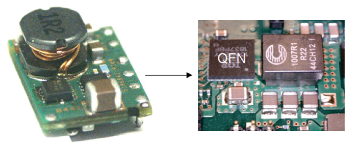
Figure 2. Voltage regulator package migration.
Regardless of application, new QFN packages need to be designed with thermal and power dissipation requirements in mind. Overpowering or overheating a device can lead to internal package failure or downstream device errors.
To help ensure adequate thermal and power dissipation, QFNs are designed to be soldered to a thermal pad located under the device connecting the PCB and component exposed die paddle (Figure 1). Within the thermal pad area, thermal vias are connected to sub-surface power/ground layers completing the heat/power sink structure for the device. During operation, the QFN generates heat. FIGURE 3 shows various heat flux paths, including radiation from the package body, conduction through the bulk PCB, and conduction through thermal vias. By design, the majority of heat is intended to be transferred using via-in-pad (VIP) structures.
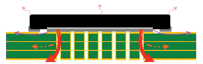
Figure 3. Heat transfer using PCB thermal pad.1
The resulting thermal VIP structure is very efficient. It provides greater design flexibility and low thermal resistance in a standard size device package. Superior electrical and SI characteristics are obtained due to minimal lead lengths, reducing electrical path distances between the silicon die and PCB.
While QFNs have been incorporated into consumer and mobile electronics for some time, these packages are now making their way into enterprise server and storage products. Original QFN VIP design points suitable for consumer grade electronics may not be suitable for higher-complexity, high-reliability products.
PCB design guidance for QFN thermal pads, thermal vias and I/O can be found in IPC-7093, Design and Assembly Process Implementation for Bottom Termination Components, issued March 2011.2 Component supplier guidance is also available to help ensure designs meet supplier requirements for optimal package operation.1,3,4,5,6,7,8,9,10,11
Upon review of the design guidance documentation1-11, two primary design points dominate. QFN thermal pads are recommended to have thermal vias either filled or left as open copper through-hole vias. Filled vias are achieved either by via tenting or using VIPPO technology. Via tenting covers thermal through-hole vias using conventional solder mask (top or bottom). Via-in-pad plated over (VIPPO) technology fills thermal vias with conductive epoxy, then caps them with copper (FIGURE 4).
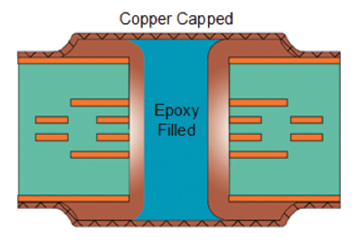
Figure 4. VIPPO basic structure.12
While via tenting and VIPPO techniques may be suitable for some applications13,14,15,16, they are not necessarily acceptable for others. Tenting vias with solder mask has been known to increase the risk of long-term PCB reliability issues such as insulation resistance failure, plus other mechanisms. Additionally, VIPPO can add 15 to 20% to the PCB fabrication cost, and suppliers of high-quality PCBs are limited. VIPPO application is also limited by PCB thickness, generally ranging from 0.040" to 0.110" stackups. VIPPO use beyond this range has not been widely assessed for long-term reliability.
Open copper through-hole thermal vias are unprotected solderable vias found within the thermal pad area under the QFN (FIGURE 5). In this case, solder paste deposits are printed on the PCB thermal pad, avoiding through-hole via locations. Upon reflow, printed deposits will flow, outgas and connect with other nearby deposits. The intent with this design point is to create a PCB thermal pad structure that is completely soldered to the exposed QFN die paddle, maximizing the thermal connection area under the package.
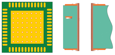
Figure 5. Open thermal through-hole via structure.1,12
In practice, numerous issues have been identified using this approach, including:
- Solder wicking down thermal vias
- Component standoff variation (tilting, floating)
- Increased thermal pad voiding levels
- Backside solder protrusions exiting thermal vias.
If thermal vias fill with solder during reflow, this can limit QFN population to a single-sided printed PCBA, increase rework difficulty, promote additional operator touch-up operations, and can leave dangerous solder shards that may become a shorting risk.
An alternate thermal pad design option is discussed focusing on next-generation QFNs with package body sizes ranging from 1 to 4mm2. The new design point is independent of board thickness and can be used on PCB stackups ranging from 0.040" to 0.250".
The work outlined here includes component symbol changes to 124 unique part numbers, nearly 300 placements, and multiple QFN component suppliers across multiple server and storage class hardware systems.
Intent and Objectives
The intent of this work is to offer a new design point option using QFN packages beyond what is currently recommended by IPC-70932 and component supplier guidelines.1,3,4,5,6,7,8,9,10,11
There were five objectives:
- Provide new design guidelines for an alternate QFN VIP option using standard PCB through-hole via and solder mask technologies in combination with conventional SMT solder stencil technology.
- Enable a solution that can be used across a wide variety of BTC package types, PCB stackups, and assembly/rework process windows.
- Enable high-quality and -reliability QFN performance integrating assembly, thermal, power and signal integrity specification requirements.
- Enable a repeatable automated hot gas rework process, minimizing the need for subsequent operator touch-up using additional flux and hand soldering iron.
- Provide a cost-effective alternative to VIPPO thermal via design points.
As described by T. Adams et al17 and IPC-7093,2 there are a number of parameter inputs to consider when optimizing a QFN design:
- Thermal pad and I/O dimensions
- Thermal vias (quantity, size, pitch, location, and type)
- Solder mask coverage (thermal pad and I/O)
- SMT solder stencil apertures (A/R and solder volume).
Monitored output responses include:
- Component standoff (reliability)
- Thermal pad % coverage (thermal/power dissipation)
- Solder voiding levels (thermal pad and I/O)
- Solder wicking down thermal vias
- I/O opens/shorts.
The challenge with QFN printed circuit design is balancing assembly/rework, power, thermal and SI requirements to sufficiently dissipate heat and electrical current while ensuring the device is easily manufacturable.
The first step in any design is to review and understand the component supplier’s specifications and guidelines for a particular device. Requirements for via quantity, thermal duty, operational power, current requirements and signal integrity will be specified.
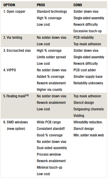
To date, five primary design options have been recommended by IPC-7093 and component supplier guides. FIGURE 6 illustrates each option using a nine thermal via layout. TABLE 1 lists associated pros/cons for each option. In addition, a new option (#6) is provided resulting from the work within this study. This new option is considered a progression of learning, utilizing the best practices used across options 1-5, and extending concepts for next-generation designs, where scale continues to shrink.
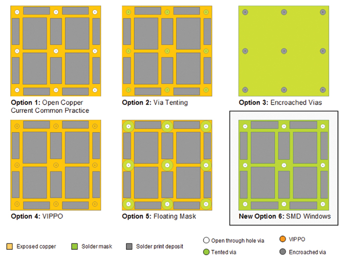
Figure 6. QFN thermal via design options.
Table 1. Thermal Via Option Pros and Cons
Current Industry Practice
Design options 1, 2 and 4 shown in TABLE 1 have been widely implemented2,13,14,15,17,19,20,21 over the past 10 years with varying degrees of success.
With regard to Options 2 and 4 above, IPC-70932 recommends plugging thermal vias (Section 6.1.3.5): “It is important to plug the via to avoid any solder wicking inside the via during the soldering process.” For enterprise server and storage applications targeted within the scope of this study, via plugging in the form of solder mask tenting is not permitted. Concerns with long-term PCB reliability remain an issue. VIPPO-based designs, while helpful in eliminating solder wicking down vias and enabling larger process windows, are expensive and are not fully tested on thick PCB stackups >0.160". Questions with long-term VIPPO barrel pad stack reliability remain.
Open copper thermal pad/via designs (Option 1) are most commonly used, and were the starting point for this study. Solder wicking variability (FIGURE 7) was shown to be the most significant issue using this design point.
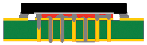
Figure 7. Thermal via solder wicking variability.1
In some cases devices soldered to open copper thermal via structures worked very well, with minimal solder wicking, low thermal pad voiding, and minimal back-side via solder protrusions. In other cases devices soldered using the exact same approach were not acceptable. Reducing part-to-part variability across a variety of PCB stackups by controlling the design point was the key lesson learned during early trials using open copper thermal pads.
Several key observations using this approach were noted during early study and are described below. FIGURE 8 shows a sample five via open copper thermal pad/via structure and associated SMT solder stencil print layout that was evaluated. The first area of concern noted was solder intended to connect the PCB thermal pad, and device die paddle was wicking down thermal vias (FIGURE 9). Robbing the thermal pad of solder can lead to intermittent grounding and device failure, increased voiding, lower effective % coverage, and lower standoff/reliability for the device.
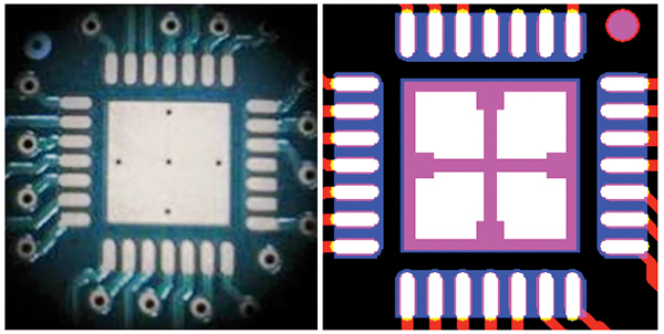
Figure 8. Starting design point: open Cu thermal pad.
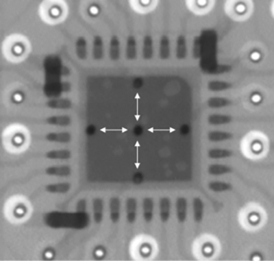
Figure 9. Solder in thermal vias.
Depending on the PCB stackup thickness, back-side solder protrusions were observed (FIGURE 10). The protrusions were found to be a function of the thermal pad size and PCB stackup. The larger the thermal pad and thinner the PCB, the more protrusions observed. Such protrusions can lead to back-side assembly/rework issues, signal shorting, power/ground shorting, and can introduce conductive solder shards to the system, should a shard break free from a via annular ring.
Figure 10. Solder protrusions.
Inadequate thermal via quantity was another significant observation with early design reviews. If there are not enough vias included within the thermal pad area (FIGURE 11), heat transfer into sub-surface ground layers will be limited and may result in the device overheating (and possibly failing) during operation. Low via counts can increase electrical impedance to ground, affecting device power and SI performance.
Figure 11. Inadequate via quantity.
IPC-7093 (FIGURE 12) includes guidance on the number of thermal vias to include within a thermal pad to sufficiently transfer heat from a device into the PCB. The figure summarizes work completed using 12mil FHS (finished hole size) thermal vias, a variety of via patterns, using a large 9 x 9mm package – examining via counts and effective heat transfer. All vias are connected directly to ground/power planes with no thermal relief structures present.
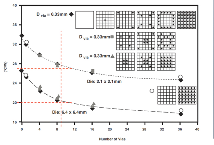
Figure 12. IPC-7093-6-12 via count thermal effects.2
As the results from the legacy March 2011 study show, use of nine thermal vias offered optimal heat transfer efficiency. While heat transfer improvements may only be marginal when adding more than nine vias, keep in mind additional vias may be required for other reasons, including power dissipation and SI needs.
The next observation relates to I/O pins on QFN devices. Voltage regulation is a common application for this device type. Therefore, circuit designs often integrate surface power and ground shapes as shown in FIGURE 13. If the component symbol is not designed to include solder-mask-defined (SMD) I/O pins, then ganged opening areas will occur as denoted by the arrows in Figure 13. Since there is no solder mask in these ganged area openings, adjacent I/O solder joints have been shown to flow and bridge together during reflow. Although this has minimal power/ground electrical impact, this is considered an IPC-61023 defect per section 5.2.7.2. These bridged solder joints can in turn reduce overall second-level interconnect reliability. It is therefore recommended SMD I/O copper pad geometries be used.
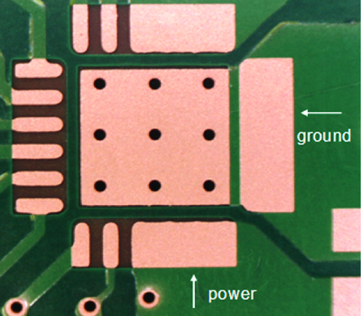
Figure 13. Ganged solder mask I/O openings.
The fifth observation relates to thermal via placement. FIGURE 14 shows an example layout using 10 vias. The image on the left shows top side thermal via placement only. At first glance all locations appear random. When copper etch layers are revealed (right image), however, it can be seen that six of the vias were located for close proximity wiring of nearby I/O grounding pins. The remaining four vias were not wire-routed and were connected only to sub-surface power/ground layers. They were placed in random locations within the thermal pad area.
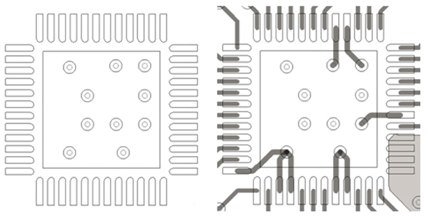
Figure 14. Random via locations.
Random via placement, as illustrated, relies on via plugging methods (tenting or VIPPO). If either of these methods is unacceptable for a particular application, as is the case within this work, then solder stencil aperture design is made much more difficult. Balancing thermal pad % coverage and minimum stencil aperture ratios, while avoiding open thermal vias, is extremely challenging and may not be possible in some cases. Non-symmetric solder deposits on the thermal pad can lead to other problems as well. Components have been observed to skew, float, and/or tilt, causing I/O shorts and opens, reducing overall first pass assembly yields. It is therefore recommended thermal via placement follow standard x/y grid arrays and avoid random placement.
Alternate SMT stencil printing methods also have been observed. “Zebra printing” patterns as shown in FIGURE 15 have been used with the intent to avoid printing solder down vias, permit proper outgassing channels to reduce voiding, and ensure adequate thermal pad solder coverage.
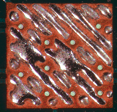
Figure 15. “Zebra printing.”
Unfortunately, resulting constructions using this approach have not been very effective and not well controlled. Minimum % solder coverage violations (<50%), increased stencil aperture clogging/reduced throughput, and via solder wicking have all been reported. As a result, alternate stencil printing methods such as Zebra printing patterns are not recommended to help reduce part-to-part thermal pad print variability.
New Design Point Considerations
Based on extensive learning using open copper thermal pad/via constructions, a new design point option was developed with the intent of improving/eliminating as many highlighted issues from earlier study. The new approach incorporates solder-mask-defined windows within the thermal pad area and I/O leads as illustrated in FIGURE 16.
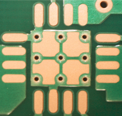
Figure 16. SMD window design option.
There were multiple goals with the new approach, including:
- Utilize low-cost open through-hole via structures
- Eliminate solder wicking down thermal vias
- Ensure proper via counts to manage heat/power
- Maximize thermal pad % coverage with solder
- Reduce standoff variability; improving reliability22
- Provide proper ground return paths, ensuring long-term electrically stable system operation
- Enable safe, repeatable rework process windows.
Design rules shown within TABLE 2 apply to BTCs in the form of QFN, MLF, MLPD, MLPM, MLPQ, VQFN, and DFN, as well as FETs and MOSFETs. Guidance is provided to enable lead-free RoHS-compliant constructions, offering high-quality, high-reliability enterprise server and storage class products.
Table 2. SMD Window Design Parameter Ranges
As described in Table 1, numerous benefits are associated with this approach. Combining conventional through-hole vias with custom solder mask windows within the thermal pad area is the essence of the design. This simple approach not only has technical benefits, but commercial procurement benefits as well. Integrating qualified through-hole via and solder mask technologies enables more PCB suppliers to fabricate cards with this design, which in turn helps spread demand over a wider supply base, and helps lower the overall cost of the solution.
The use of SMD windows helps reduce part-to-part variation in multiple ways. Since solder cannot travel down vias, thermal pad standoff (post-reflow) is more consistent; voiding levels are reduced since solder is not being robbed from the thermal pad, and solder-mask-defined out-gassing channels are embedded. Symmetrical solder pad print layouts minimize component tilting or skewing during reflow, reducing I/O shorts and opens risks. The result is more effective thermal and power management of the device, with a high level of thermo-mechanical reliability.
Another benefit to this approach is the design’s wide application window. Using 8/10/12mil FHS through-hole vias with solder mask can enable SMD window designs spanning PCB thicknesses of 0.040" to 0.250". Via plugging options are aspect-ratio-dependent and cannot offer this range.
The design also enables a safe and high-quality rework solution. With solder not able to travel down vias, component removal and site redress operations are simplified. Risk of backside solder protrusions during defective part removal is eliminated, reducing the need for dangerous operator hand-iron touch-up actions. Use of standard 6mil solder mask webs helps ensure solder mask peeling does not occur during site redress.
Results and Discussion
Common SMD window layouts are generally defined as having via counts ≤9. Examples of some common layouts are shown in FIGURE 17.
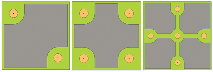
Figure 17. Common SMD window layouts (not to scale).
The same SMD window approach can be used for more complex layouts as well. These are defined as via counts ranging from five to 31 (or greater) within the thermal pad area. Examples of some more complex layouts are shown in FIGURE 18.
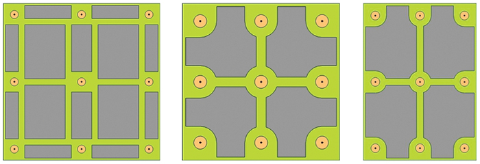
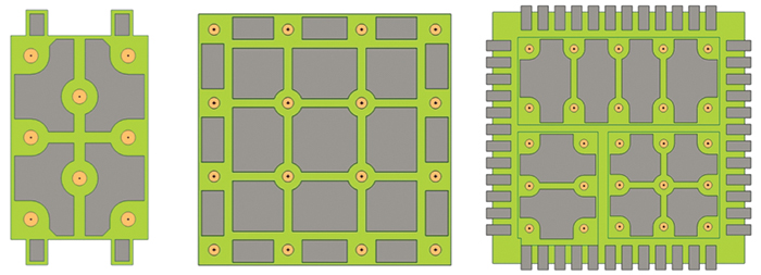
Figure 18. Complex SMD window layouts (not to scale).
As with any design point key parameters must be well understood and controlled to enable ease of manufacturing/reworkability and achieve high-quality/reliable device operation over the life the system. As such, the following sections discuss key challenges to manage when implementing new SMD window designs.
Qualified via sizes and minimum pitch. With the migration to elevated lead-free processing windows, it is critical qualified laminate materials be used in combination with qualified via sizes and pitches. Design layouts will change depending on the application PCB stackup, determining what via/pitch options can be safely and effectively used.
SMD window layouts can be designed using 8mil FHS vias on 0.8mm (32mil) via pitch and 6mil solder mask webs for card stackups ranging from 0.040" to 0.160". If thicker PCB applications are necessary (0.160" to 0.250"), the use of 10mil or 12mil FHS vias may be required.
Be aware that using orthogonal via arrays introduces signal wiring limitations. If nearby wiring densities are high, routing sub-surface under BTC thermal pad via arrays will be very limited. Majority routing will need to occur outside the device keep-out area. Wireability is yet another factor to consider when selecting via counts during the design phase.
It is important to balance thermal via quantities required by the supplier with thermal pad solder % coverage, while ensuring solder does not wick down vias. As thermal via counts increase and thermal pad areas decrease, this reduces the available % solder coverage connecting the device to the PCB. Stencil aperture ratios (A/Rs) must closely be monitored to ensure consistent solder deposits are printed. In some cases where the via quantity cannot accommodate minimum % coverage requirements within the thermal pad, some vias may need to be placed outside the component outline as “outriggers,” shown in FIGURE 19. Although this may not be the best thermal solution (increased conduction path), vias may still be required for power and SI management reasons.
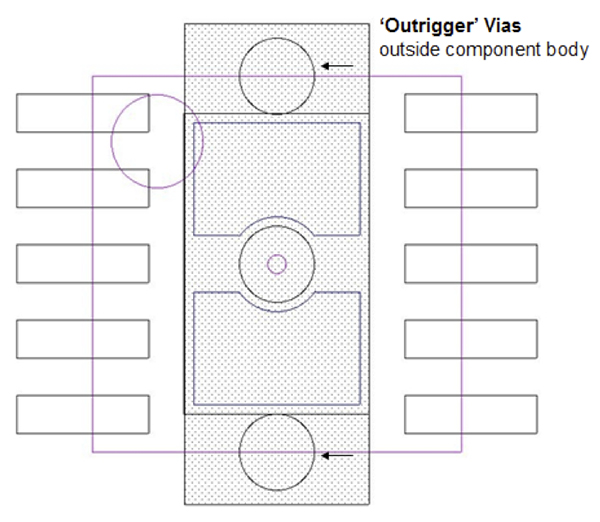
Figure 19. “Outrigger” thermal vias.
Solder mask alterations. A key learning from implementation efforts is to ensure PCB suppliers are not modifying solder mask web designs per the original design file to accommodate internal process capabilities. IPC-70932 permits use of 3mil solder mask webs; however, not all PCB fabricators have this capability. The use of 6mil solder mask web used in this design point is considered standard technology; there is no reason for additional modifications to be made by PCB suppliers. FIGURE 20 shows an open copper thermal pad structure resulting from solder mask removal by the supplier. It is therefore important to review and verify actual PCB constructions produced by the PCB supplier to ensure desired thermal pad structures are formed.
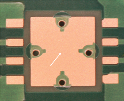
Figure 20. PCB supplier removal of solder mask web.
SMT stencil alterations. PCB copper shapes should be designed with stencil aperture ratios (AR) in mind as outlined in Table 2. SMT Stencil aperture openings should be designed 1:1 with copper thermal pad shapes and I/O pads. FIGURE 21 shows an example of where significant SMT stencil aperture modifications were made by a contract manufacturer. Resulting thermal pad print deposits do not match copper windows. Low % coverage, solder via wicking, signal opens, and increased risk of intermittent ground failures have been reported with such drastic modifications.
Figure 21. Solder deposits not 1:1 with Cu pad.
In some cases, aperture reductions from 1:1 Cu geometries may be required by the assembler to help with printing registration, solder slump, or other assembly line specific needs. As shown in FIGURE 22, such aperture reductions are acceptable to meet manufacturer capabilities, but need to be optimized and verified accordingly. Gray areas shown in the figure are solder print deposit areas; orange areas are PCB copper pad areas.
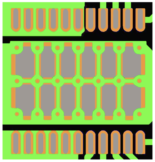
Figure 22. 1:1 stencil aperture reductions.
During early manufacturing stages, it is therefore important to verify that SMT stencil design windows match PCB copper thermal pads and I/O. If 1:1 reductions are required by the assembler, optimization and verification are required.
Thermal pad voiding. IPC-70932 Section 6.1.5.3 gives the following guidance for voiding within thermal pads: “The presence of small voids in the thermal pad region is not likely to result in degradation of thermal and electrical performance, nor impact the reliability of perimeter I/O solder joints.” Based on this and published component supplier guidance, the goal with the SMD window design was to minimize large coalesced voids and target 30% maximum voiding as measured by cross-sectional area. Note the current limit set by IPC-7093 is 50%.
As reported in numerous studies14,15,16,17,24,25,26, several factors affect voiding, including the number of thermal vias, size of thermal pads, and outgassing channel allowance. The SMD window approach helps minimize voiding levels by incorporating solder-mask-defined outgassing channels, combining numerous small thermal pads instead of one large opening, and does not permit solder to be printed down vias. These features work together to manage voiding to within acceptable levels. The design also helps minimize violent outgassing that can lead to excessive solder balling, leaving solder shards behind, increasing shorting risks. FIGURE 23 shows sample voiding levels when using this approach. The figure shows voiding levels are within acceptable limits, but further optimization may be required to reduce levels even further. Reduction of voids helps increase effective % coverage of the thermal pad connection and should be a continued focus item to refine the SMD window approach.
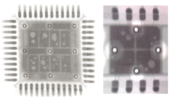
Figure 23. Thermal pad voiding examples.
Implementation status. To date, the SMD window design approach has been applied to over 124 unique physical symbols, affecting over 296 unique part number placements spanning a wide variety of enterprise server and storage systems. Component function includes power regulation, logic controller, and clocking devices.
FIGURE 24 shows the pareto distribution of usage for all part numbers implemented. While a few devices are used across multiple card designs, the pareto shows the variety of different components on the market and their niche uses within circuit designs. This clearly illustrates the significant increase in adoption rates of these device types within server and storage class hardware.
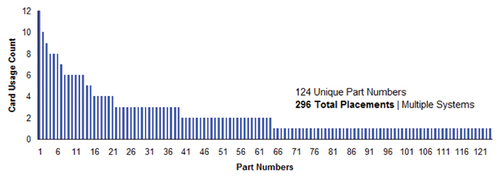
Figure 24. VIP implementation pareto summary.
FIGURE 25 shows resulting via count usage and % coverage obtained on SMD window implemented devices. The majority of vias used across all designs ranged from four to nine, with some applications requiring as high as 31. Thermal pad % coverage for all devices ranged from 63 to 74%.
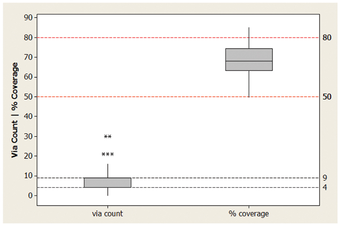
Figure 25. Via count ranges and resulting % coverage.
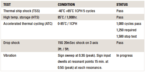
Interconnect reliability testing performance. At the time of publication, reliability testing of the design point is still in progress. Test results obtained to date are encouraging, proving the design point offers a reliable solution over the longer term. Results are shown in TABLE 3.
Table 3. SMD Window Reliability Test Results to Date
Summary
While IPC-7093 and component supplier guidance documents continue to provide valuable guidance on how best to design and manufacture card assemblies using BTCs, there has been significant growth in BTC usage in more complex constructions over the past three years.
A greater variety of device packages are being introduced into higher complexity, high-reliability server and storage class hardware using thermal pad structures. Package sizes continue to shrink; many are now less than 3mm2 (well beyond 7mm2 data found within IPC-7093). Component placement counts are significantly increasing; in some cases 10 to 20X placement density over legacy product designs have been reported. Increased device functionality is continually drawing more power, as well as producing more heat that must be dealt with.
With all of these factors in mind, a new SMD window design option was established. The design builds on best practices from IPC-7093, supplier design guidance documentation, and legacy industry literature. Extension into smaller form factor BTC devices with higher placement densities and greater thermal/power dissipation needs were key drivers for this design point.
Improving ease of manufacturability for primary attach and rework processes was yet another motivator. The majority of industry and supplier guidance continues to focus on primary attachment quality and reliability. The SMD window design addresses both primary attach and rework needs. It enables safe and repeatable rework process capability, with many benefits over other design options.
In summary, an alternate BTC design approach has been implemented. Key benefits include:
- Device thermal/power dissipation requirements met
- High quality/device reliability
- Improved manufacturability
- Rework consistency and safety
- Low cost, enabling larger PCB supplier base
Recommendations
Recommendations from the study include:
- A new solder-mask-defined SMD window PCB design option can be used to produce high-quality, high-reliability BTC structures in a variety of enterprise server and storage class electronic hardware.
- Update IPC-7093 (March 2011) to include packaging advancements with smaller device sizes introduced over the past three years. Include new SMD window design as an alternate option. Update rework sections to promote safe, repeatable, reliable rework operations.
- Update supplier BTC design guidance documentation to include new SMD window design as an option. It may be unacceptable to rely on solder mask tenting and/or VIPPO techniques to plug thermal vias, especially for high-dollar-value, high-reliability applications. Expand design options to better align with higher complexity product design needs and limitations.
- Integrate new SMD window designs into BTC supplier demonstration test vehicle studies. Continue building data and work to further refine the method with supporting build experience and test performance.
- Solder wicking down open through-hole vias should be avoided. Solder in vias can lead to increased thermal pad voiding, backside solder protrusions (limiting second-side assembly/rework), and greater standoff variability.
- Ensure qualified PCB laminates, via sizes, and via pitches are properly used. PCB stackup (thickness) will determine what laminate/via/pitch options can be safely and effectively used.
- Ensure proper via quantities are added to BTC thermal pad designs. Be aware that via counts are needed for more than just thermal needs, but also power and signal integrity. Be careful of applying IPC-7093-6-12 recommendations independently. Consideration of power and electrical requirements are also critical.
- Ensure thermal via placement follows standard x/y grid arrays and avoid random placement. Properly placed vias help optimize SMT stencil aperture design and solder symmetry, reducing device open/short risks and improving PCB wireability.
- Solder-mask-defined I/O is recommended to eliminate the possibility of adjacent pins bridging as is found when ganged solder mask openings are used. This is especially important for voltage regulation applications when surface power/ground shapes are used to transfer power through the device. Cingulated I/O helps improve overall thermo-mechanical reliability performance of the package over the longer term.
- Balancing solder % coverage and SMT stencil aperture ratios is critical to achieve an acceptable SMD window design point. Power/heat transfer efficiency depends on a balanced thermal pad structure.
- Closely monitor PCB suppliers to ensure solder mask web alterations (or other changes) are not being made beyond data contained within original design files.
- Closely monitor assembly partners to ensure SMT stencil aperture alterations are not made beyond data contained within original design files. If reductions are necessary for a particular application, review and verification effort is required.
- Continue to monitor and evaluate thermal pad voiding impacts to device function for long-term reliability. Continue driving acceptable voiding limits down from 50% to 30% or less.
Acknowledgments
The authors would like to thank colleagues Jim Bielick, Dave Boser, Willie Davis, Donald Heintz, Justin Henspeter, Phil Isaacs, Jordan Keuseman, Roger Krabbenhoft, Theron Lewis, Larry Pymento, Pat Sobotta, Jeff Taylor, and Timothy Younger for their significant contributions to this work.
Ed.: This article was originally published at SMTA International Conference in October 2014 and is republished here with the authors’ permission.
References
1 Cirrus Logic, Thermal Considerations for QFN Packaged Integrated Circuits AN315REV1, July 2007.
2. IPC-7093, Design and Assembly Process Implementation for Bottom Termination Components, March 2011.
3. Texas Instruments, Texas Instruments QFN Layout Guidelines – HPL Audio Power Amplifiers, Application Report SLOA122, July 2006.
4. Texas Instruments, PowerPad Thermally Enhanced Package Application Report – SLMA002G, January 2011.
5. Atmel, QFN Package Mounting Guidelines AT88RF1354 Application Note, March 2009.
6. Carsem, MLP Micro Lead Package Application Note, April 2002.
7. Freescale Semiconductor, PCB Layout Guidelines for PQFN/QFN Style Packages Requiring Thermal Vias for Heat Dissipation AN3778, Rev 0.2, 2010.
8. International Rectifier, Power QFN Technology Inspection Application Note AN-1137, Version 1.0, June 2008.
9. Lattice Semiconductor, PCB Layout Recommendations for Leaded Packages Technical Note TN1257, October 2013.
10. ON Semiconductor, Soldering and Mounting Techniques Reference Manual SOLDERRM/D Rev 7, June 2012.
11. Renesas, QFN Mounting Manual R50ZZ0005EJ0100 Rev. 1.00, September 2013.
12. IPC-6012C, Qualification and Performance Specification for Rigid Printed Boards, April 2010.
13. A. Syed and W. Kang, “Board Level Assembly and Reliability Considerations for QFN Type Packages,” SMTA International, September 2003.
14. D. Herron et al, “Voiding Control at QFN Assembly,” SMTA International, October 2011.
15. D. Herron, et al, “The Effect of Thermal Pad Patterning on QFN Voiding,” SMTA International, October 2012.
16. B. Sandy-Smith, “Reliability Challenges for Bottom Termination Components,” International Conference on Soldering and Reliability, May 2013.
17. T. Adams, “Considerations for QFN Thermal Pad Solder Coverage,” SMTA International, October 2011.
18. L. Li, et al, “Board Level Reliability and Assembly Process of Advanced QFN Packages,” SMTA International, October 2012.
19. S. Sytsma and M. Wrightson, “Lead-Free Solder Durability Testing at Accelerated Thermal Excursions for QFN and DFN Package Interconnects,” SMTA Pan Pacific Symposium, January 2007.
20. D. Xia, et al, “Mechanical Reliability and Thermal Design Studies of QFN Packages,” SMTA International, October 2007.
21. R. Otte, “QFN Manufacturing: Configurations, Materials and Processes,” SMTA International, October 2009.
22. D. Kim, M. Ahmad and S. Teng, “Reliability Study of Lead-Free SnAgCu Solder Joints vs. SnPb Solder Joints in QFN Packages,” SMTA International, September 2006.
23. IPC-A-610E, Acceptability of Electronic Assemblies, April 2010.
24. Z. Feng, et al, “How to Resolve Defects Related to Pad Design with the aid of Non-Destructive and Destructive Methods,” SMTA International, October 2009.
25. D. Bernard, et al, “Common Process Defect Identification of QFN Packages using Optical and X-ray Inspection,” SMTA International, October 2007.
26. S.Chen, et al, “Using SPI, AXI, and CT X-Ray Data to Improve SMT Process with QFN Devices,” SMTA International, October 2012.
Matt Kelly, P.Eng, MBA is senior technical staff member | senior inventor, IBM Systems, Global Hardware Execution; Mark Jeanson is engineer at IBM Global Services, and Mitch Ferrill is senior engineer at IBM; This email address is being protected from spambots. You need JavaScript enabled to view it..


