

And why waiting until the last process step is a bad idea.
BTCs, or bottom termination components, are a class of package referred to by a variety of acronyms and abbreviations. Different component and packaging companies may use different nomenclature (FIGURE 1), but almost all these components share one common, ugly characteristic: large pads that are prone to solder voiding. By design, these large thermal or ground pads require a defined percentage of contact with the solder and PCB to properly conduct heat and/or electricity. Excess solder voids can impact performance and reliability of the package.

Figure 1. Multiple names of BTCs.
The voiding problem has given both designers and manufacturers heartburn for the better part of two decades. Some of the drivers for this frustration are that voiding rates are highly variable, and numerous factors can impact their formation. While there is still no clear consensus on how much voiding is acceptable, one trend is clear: the smaller and fewer the voids, the better. Voids cannot be completely eliminated, but there are a number of ways to minimize their formation, ranging from PCB design and solder paste formulation to stencil design and reflow profile adjustments.
PCB design. Large “lake” voids can be averted by dividing the large pad with solder mask (FIGURE 2). Using solder mask to create “window panes” (as shown on the left) maintains outgassing paths for volatiles to escape, and often prevents smaller voids from merging together into larger ones (as shown on the right). If contact area is critical to the function of the device, the solder mask-covered areas obviously do not have the opportunity to make contact with the solder, and the design calculations should reflect the limitation of the masked areas to conduct heat or electricity, in addition to anticipating a certain amount of voids in the solderable areas.

Figure 2. BTC center pad divided by solder mask to limit void size.
Additionally, if the pads contain thermal vias, voiding can be mitigated by not applying solder mask or solder paste over the vias. Leaving the vias unobstructed provides outgassing paths through the PCB (FIGURE 3).
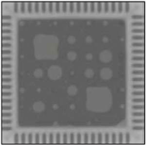
Figure 3. Ground pad “window pane” solder mask design and effect on void size.
Solder paste selection. Solder paste formulations balance a large number of characteristics, including reliability, wetting, pin-testability, printability, shelf life, cleanability and reflow properties. Balancing all these considerations will have an impact on paste voiding characteristics. Selecting a solder paste formulated to mitigate voids in the reflow process will result in smaller and fewer voids not only under BTCs but in BGAs and other components as well.
Solder paste consists of two components: flux medium and solder powder. The role of medium on solder void formation can be manipulated using various techniques, including solvent selection and activator systems. We set out to determine if size and distribution of the spheres in the solder powder would have any impact on BTC void formation. If we could correlate powder distribution to void reduction, we would be able to offer another tool to the assembler toward void reduction. Unfortunately, the initial test results do not indicate a strong correlation between voiding and particle size distribution; however, the research continues to explore the relationship in greater depth. We’ll keep you posted on our findings.
Stencil design. We recently completed a series of designed experiments on void generation using the AIM standard test vehicle, which contains a variety of BTC footprints. (Users wishing to use this board in their own tests can get it from Practical Components.) We were able to try 18 different stencil aperture designs and coverage ratios (FIGURE 4). We found that voiding is not as dependent on paste coverage area percentage as it is on the design of the apertures. Our data indicate designs that created outgassing paths for flux volatiles outperformed designs that did not.
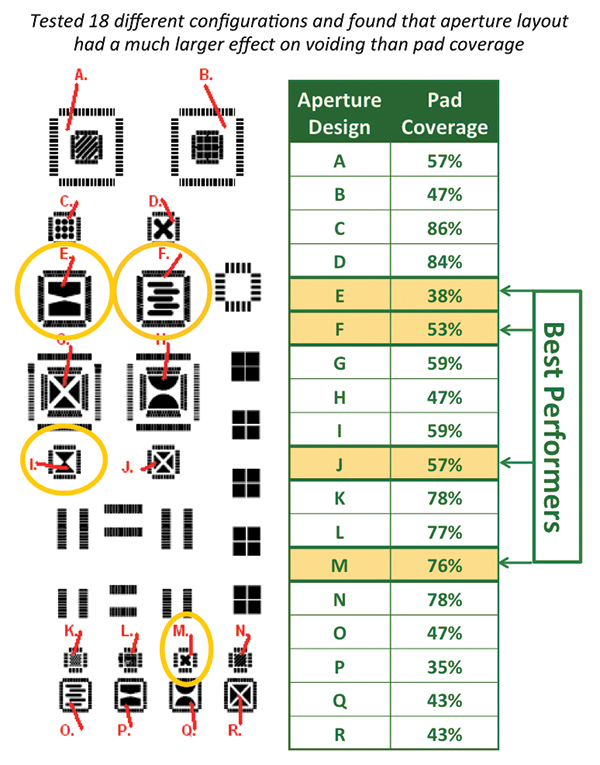
Figure 4. Center pad aperture design experiment.
BTC stencil design should consider component “float” in addition to voiding. Printing excess solder paste on the center pad can create a large solder mass that is taller than the adjacent solder masses on the component lands. During reflow, the BTC component floats or tilts/skews on the surface of the large liquid central solder mass, creating open or unreliable solder joints on one or more sides of the device. As a general rule, if any of the terminations’ stencil apertures have area ratios less than 0.75, the stencil designer should perform some basic calculations on the solder volumes and relative heights of the I/O joints versus the center pad. Ideally, the solder joints on both should have standoffs of 2 to 3 mils.
Reflow profile. Our experiment tested five different reflow profiles, which varied peak temperatures from 240° to 255°C, time above liquidus (TAL) from 50 to 90 sec., and time to peak temperature from 3:30 to 5:30, in both straight ramp and soak configurations. We found that the best (lowest) voiding performance was obtained with lower peak temperatures and shorter TAL. High peak temps and long TAL created the most voids. Soak zones did not exhibit a profound effect on voiding behavior. FIGURE 5 compares center pad voiding results of the best- and worst-performing profiles.
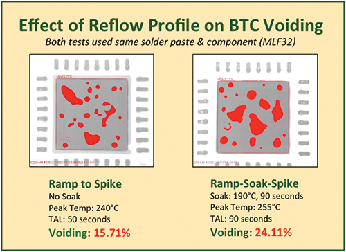
Figure 5. Reflow profile effect on voiding.
BTC voiding will never be completely eliminated, but it can certainly be mitigated at numerous points in the product development cycle. PCB designers can apply void-limiting layout strategies like “window paning” the thermal and ground pads with solder mask, strategically placing thermal vias and leaving them unobstructed, and consulting with their assembler. Either the designer or assembler could specify low-voiding solder paste. Prior to production, the stencil designer can maintain outgassing pathways created by the solder mask divisions, or create pathways if solder mask divisions don’t exist, and keep solder paste away from vias. Finally, on the production floor, the process engineer or technician can often tweak the reflow profile to reduce void formation.
Unfortunately, that last line of defense – the production floor – is used as the first line. At that juncture, a great deal of opportunity to limit voiding has already been missed. The only tools the assembler has are:
- Solder paste selection, if not specified by OEM.
- Aperture redesign.
- Reflow profiling.
These variables, even in combination, have limited and changeable impact on void reduction. If BTC voiding raises concerns about electrical or thermal performance, the most effective measures can easily be taken early in the PCB design process to address it throughout the development and introduction of the product. Each individual strategy contributes to improved contact, and the more deployed, the better the results.
Karl Seelig is vice president of technology at AIM Solder; This email address is being protected from spambots. You need JavaScript enabled to view it.. Tim O’Neill is regional manager at AIM; This email address is being protected from spambots. You need JavaScript enabled to view it..


