No industry trends stayed secret at ECTC in Las Vegas.
In early June, almost 900 people gathered in Las Vegas at the Electronic Components and Technology Conference – not necessarily to seek fortunes in the casinos, but to roll the dice on the next big trend in the electronics industry. Bet correctly on the right packaging and assembly trend, and revenues will multiply; bet wrong by installing capacity for a technology not in strong demand, and you could lose it all. Given ASE COO Dr. Tien Wu’s prediction of less than double-digit growth on the semiconductor side, the backend packaging and assembly projects to where the action will be.
Get med. The World Health Organization predicts that by 2025 more than 1.2 billion people will be over 60 years old. Given such projections for an aging population, medical electronics has tremendous growth potential. In the field of imaging, the US market is somewhat saturated for equipment providing CT scans, ultrasounds, x-rays and MRI, but portable medical devices such as defibrillators and portable ultrasounds are experiencing strong growth. Increased demand for implantable devices is anticipated for infusions, pumps, pacemakers, and even drug delivery systems. For these systems, miniaturization is key, and lessons from today’s handhelds segment may be applicable. One critical difference is that, when one drops a cellphone and it stops working, one might be unhappy, but if a pacemaker stops working, the user could be dead. Here, reliability cannot be understated. With many components only available with Pb-free finishes, companies must determine what strategy will be best to mitigate any issues. Greater use of conformal coatings, underfill materials, and encapsulants is anticipated.
Mobile architectures. The convergence of computing and communication is clearly seen in the mobile devices of today and tomorrow. Key themes discussed in this year’s ECTC plenary session focused on mobile processing architectures. The demand for increased mobility, multimedia functions, connectivity, and bandwidth is driving new technology and infrastructure developments. Companies such as RIM are increasingly focused on incorporating in smartphones’ new features such as multimedia, navigation, games, social networking, and productivity enhancements. While many of today’s smartphones use package-on-package (PoP), roadmaps include the possibility of 3D through silicon via for memory and processors. Cost remains a major focus in the adoption of any new package architectures. The introduction of Apple’s iPad calls into question how future products will be designed – starting not with the semiconductor and board layout, but instead with the user interface, screen, touch pad, and battery life.
Bright lights. With government mandates for the switch to LED lighting, the market for high brightness LEDs is expected to grow. Packaging and assembly of high brightness LEDs is increasingly recognized as critical in reducing product cost and enabling reliability. Packaging has to satisfy requirements for form, fit and function, but must also provide a conductive thermal path for the heat and meet requirements for optics. Improper heat dissipation can degrade materials and impact the performance of the luminaries. Lighting applications will provide an exciting area as engineers solve challenges with material interactions.
3D TSV. The industry clearly has moved from “PowerPoint engineering” to the hard work and challenges of materials science and real engineering in 3D through silicon via. More than 50 of the approximately 323 papers at ECTC discussed 3D TSV, with most discussing process improvements. Over the next year, companies and research institutes will be saying less and doing more to resolve manufacturing issues and challenges associated with moving from R&D projects into commercialization. Improving yield is critical to meeting cost-reduction goals. Reliability data should be forthcoming if development targets are met.
Assembly trends. With the price of gold hovering around $1,200 per oz., many companies are riding the wave of copper wire bonding. While there are still technical challenges, much progress is being made and cost is the driver. Examining the cost tradeoffs with each technology is becoming increasingly important.
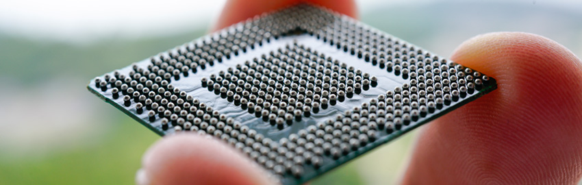
An increasing number of devices are transitioning from wire bond to flip chip. Companies are looking at finer pitch bumps and Pb-free solutions that will work with new ultra low-k dielectric materials used on the device. Many companies are interested in copper pillar as a means to reduce cost. According to STATS ChipPAC, the use of molded underfills for flip chip in strip format and designs to reduce substrate complexity have gained attention in the past year.
Wafer-level packaging remains an exciting topic, and many ECTC papers examined improved reliability for mobile applications. Small diameter balls are in production, and pitches as fine as 0.3 mm are gaining acceptance. Fan-out WLPs are shipping in volume production for high I/O parts. Capacity expansions are underway and new developments are expected as the technology is extended to stacking.
The remainder of the year promises to be exciting for the backend assembly and packaging companies. Equipment and materials sales are improving and new challenges call for closer cooperation between suppliers and users.
E. Jan Vardaman is president of TechSearch International (techsearchinc.com); This email address is being protected from spambots. You need JavaScript enabled to view it.. Her column appears bimonthly.