Designing for higher speeds and operating frequencies demands close
scrutiny to minimize the effects of unwanted energy transfer and noise
in the system.
With faster edge rates of logic devices more common, wavelengths are becoming comparable to the average circuit size. As a result, the semiconductor industry is being pushed to the limits of miniaturized component manufacturing. Even then, with speeds in the GBs range, intrinsic electrical characteristics are no longer insignificant. Many things can go wrong if sufficient thought and planning are not put into the high-speed PCB layout.
While crosstalk and ground bounce are different issues, as far as PCB design is concerned, their causes and the extent to which they may become a problem to the design are the same. Both issues are caused by intrinsic inductances and capacitances, and their criticality may increase with a rise in operating frequencies. These issues are two of the most common problems that may come back and haunt the OEM team after product launch.
Crosstalk
Crosstalk is the transfer of energy between the adjacent conductors due to capacitive or inductive coupling. In order for the crosstalk to occur, there must be an active and a passive line close together. The active line carries the signal, and the passive line is the one where ideally, no signal should be present. The electromagnetic field generated by the active line can interact, causing transient current to flow on the victim line. If the electric field interaction is dominant, the crosstalk is called capacitive crosstalk. If, on the other hand, a magnetic field is dominant, then it is called inductive crosstalk. Both types of crosstalk are unwanted, and it is the responsibility of the layout designer to keep these within the noise budget of the logic family being used in the design.
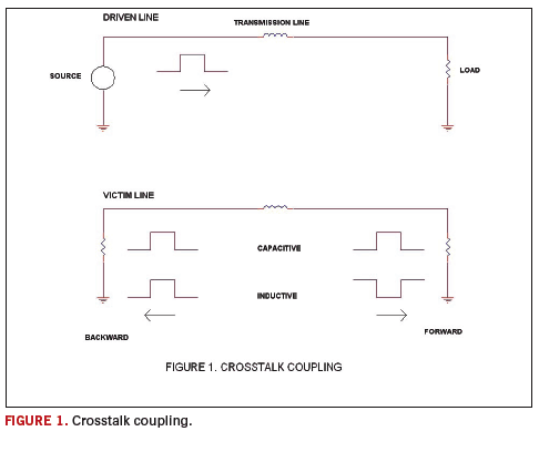
Near-end crosstalk. The signal traveling backwards toward the driver is called near-end or backward crosstalk. This type of crosstalk is measured on the victim line near the driver side of the active line.
Far-end crosstalk. The signal traveling toward the receiver is called far-end or forward crosstalk. Far-end crosstalk is measured on the victim line at the point closest to the receiver of the active line.
Capacitive crosstalk. Whenever two traces are routed parallel to each other on adjacent layers, they act as a capacitor plate pair, separated by a dielectric. Hence, this type of crosstalk is classified as capacitive crosstalk. As a side note, some amount of capacitive crosstalk will also occur when the traces are routed side by side on the same layer. However, this can be considered negligible because of the small height-to-width ratio of the traces.
Inductive crosstalk. This type of crosstalk occurs when two signals are routed on the same layer in close vicinity. It is caused by the magnetic component of the field emanating from the active line.
Consider a set of lines, as shown in
FIGURE 1. Line 1 is the active line, and Line 2 is the victim line. Crosstalk on the victim line is measured, and the coupled signal on the victim line, consisting of both capacitive and inductive components, travels in both directions.

Both capacitive and inductive crosstalk are seen at the near-end, as well as the far-end, of the victim. A critical difference, however, is that capacitive crosstalk causes the coupled signal to have the same polarity as the active signal, irrespective of at which point it is measured on the victim. The inductive crosstalk causes the signal at the driver end to have the same polarity, whereas at the receiver end, the inductive crosstalk causes the signal to have an opposite polarity as the active signal.
Since the overall coupling effect is the sum of capacitive and inductive crosstalk, near-end crosstalk is of greater magnitude, and hence, of greater concern for a PCB designer. Moreover, backward crosstalk rapidly increases with the parallel-coupled length of the two lines until it reaches a saturation point. This point is called the critical length, after which any increase in the coupled distance will make no difference.
Mathematically, the critical length is directly proportional to the rise time of the signal. Hence, effects of near-end crosstalk will increase with faster signal transitions.
Front-end crosstalk on the other hand, will show a very gradual increase with the coupled lengths of the two lines. The problem will only show up on very long parallel runs and may not cause any issues on a PCB.
Minimizing Crosstalk
As a general rule, traces routed parallel and on top of each other cause greater amounts of crosstalk than those routed side by side. Because of space constraints on modern designs, it is not possible to entirely eliminate the inductive crosstalk caused by parallel routing on the same layer. Therefore, the easiest thing a layout designer can do is to ensure that traces on adjacent layers do not route in parallel and cross at 90 degrees to each other.
For traces routed side-by-side, far-end crosstalk will only become an issue at five times the rise distance, which would be 30 inches for 1-ns rise time. However, the near-end crosstalk will increase sharply until it reaches the critical length that is around half the rise distance. Hence, for a 1-ns signal, backward crosstalk will peak at only three inches. Furthermore, the degree of backward crosstalk is the function of trace separation and the height above the reference plane. It is incumbent upon the designer to know the noise margin of the circuit being laid out.
As a rule of thumb, with digital designs having a noise margin of 10% or more:
- Trace spacing of equal to, or greater than, the dielectric separation is required in case of symmetric stripline.
- Trace spacing of twice, or greater, than the dielectric separation is required in case of microstrip.
- Decreasing the parallelism by 50% will reduce the crosstalk by 50%.
- Doubling the trace separation will decrease the crosstalk by a factor of four.
Ground Bounce
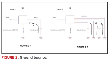
Ground bounce causes unwanted noise in the system and is more prominent with faster switching devices, or when there are more voltage swings (CMOS devices). This phenomenon can cause input glitches to the logic device and is caused by the lead inductance. Note that even the smallest of package sizes has parasitic inductances associated with its leads. Consider
FIGURE 2A.

Once output on Device A switches from 1 to 0, the load capacitor discharges. This causes a current to flow from the capacitor across the logic device’s lead. Because it has a finite lead inductance, it introduces a potential difference between the device’s internal ground and the universal circuit ground. What this implies is that the I/O of this device will be referenced to the internal ground, whereas the receiver may be referenced to the universal ground. Even though the value of this potential difference is less than the full voltage swing, it can appear as noise.
Now consider a scenario where a similar device is driving a number of outputs (see
FIGURE 2B) which are actually similar capacitive loads in parallel. If all these loads discharge simultaneously, there is a larger current through the inductive device ground pin causing more ground to bounce.
As an aside, a similar effect, known as VCC sag, occurs at the power lead of the logic device when it switches from 0 to 1. This causes the device’s VDD pin to be at a different potential than the system power rail. However, this is less of a problem because devices are generally more tolerant to input 1 than input 0.
Minimizing Ground Bounce
System level changes- Slowing down the output switching time can help reduce ground bounce. This may not be a viable solution when propagation delay is an issue.
- Multiple grounds, spread through a package and ideally located near the I/Os, can reduce ground bounce. Critical outputs, like control lines and clocks, do need to have a ground pin close by.
- Choosing a non-leaded package similar to the ones discussed below directly reduces lead inductances.
- The options for non-leaded packages include: wire-bonded package, where bond wires connect the package die directly to the board, reducing lead length; tape automated bonding, where a flex circuit is used to connect the device to the PCB, similar to wire bonding; and flip chip. This method offers the best solution for minimizing lead inductance. Solder bumps, placed directly to the device’s attachment pads, are soldered to the PCB after the device is flipped over.
- Board Level Changes
- Large power and ground planes always help by providing a low impedance path to the power system.
- A generous use of decoupling capacitors, both small and bulk, near each device’s power/GND pins will reduce ground bounce. If ground bounce is still an issue, placing small capacitors close to ground pins will assist in reducing it.
- All ground pins of the device need to be connected to the ground planes with short and wide traces. The vias should ideally be placed as close as possible to the pins, and via sharing amongst ground pins need to be avoided.
Conclusion
As manufacturers continue creating higher performance devices, issues like crosstalk and ground bounce are becoming increasingly common and harder to manage. Difficult as it may seem, these problems are manageable if ample coordination exists between the hardware engineers and the board designers, both at system level and board level. Also, sufficient time, effort and diligence needs to be put into the PCB layout so that the prototype can meet or exceed all expectations.
PCD&FSyed W. Ali, CID+, is a layout engineer with Nexlogic Technologies, Inc. For more information, contact
This email address is being protected from spambots. You need JavaScript enabled to view it..


