-
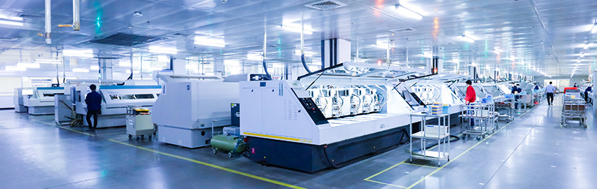
NTI-100: The World’s Top PCB Fabricators
The changing map of PCB production. READ MORE...
-
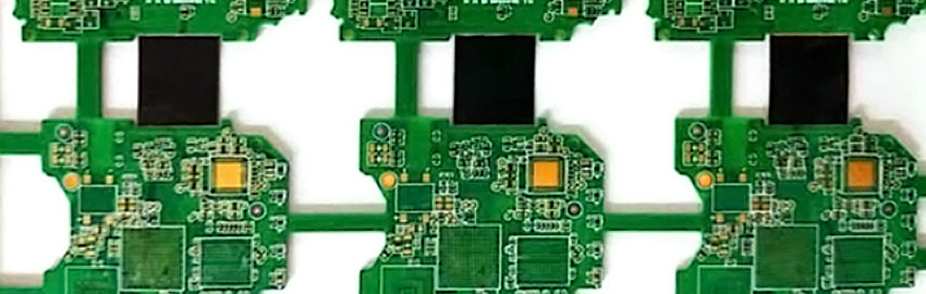
Elements of PCB Panelization
Panelize to optimize: faster builds, better boards. READ MORE...
-
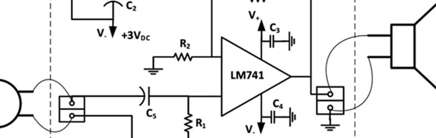
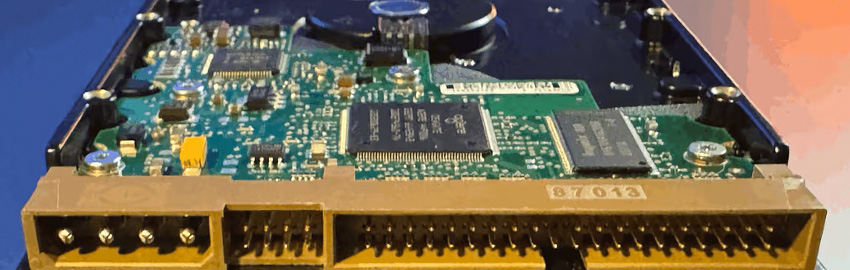
Optimizing Mixed Signal Circuit Designs
Navigating the analog and digital worlds. READ MORE...
-
Dynamic Times
Component Dynamics is where market intelligence meets distribution.
READ MORE... -
Power Circuits
Making power connections is a world unto itself. READ MORE...
-
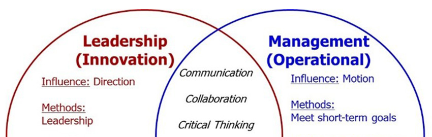
Developing Organizational Culture for Troubleshooting
Solving problems and adding value. READ MORE...
Homepage Slideshow
NTI-100: The World’s Top PCB Fabricators
The changing map of PCB production.
Elements of PCB Panelization
Panelize to optimize: faster builds, better boards.
Optimizing Mixed Signal Circuit Designs
Navigating the analog and digital worlds.
Dynamic Times
Component Dynamics is where market intelligence meets distribution.
Power Circuits
Making power connections is a world unto itself.
Developing Organizational Culture for Troubleshooting
Solving problems and adding value.


")


