State-of-the-Art Technology Flashes
Updates in silicon and electronics technology.
Ed.: This is a special feature courtesy of Binghamton University.
Generating electricity out of thin air. University of Massachusetts researchers have developed a device that uses natural protein to create electricity directly from moisture in the air, a technology that could have significant implications for the future of renewable energy, climate change, and medicine. The device is called an “Air-gen,” or air-powered generator, with electrically conductive protein nanowires produced by the Geobacter microbe. The Air-gen connects electrodes to the protein nanowires where the electrical current is generated from the water vapor naturally present in the atmosphere, literally making electricity out of thin air. The Air-gen generates clean energy 24/7 and is an exciting application of protein nano. (IEEC file #11678, UMass Amherst, 3/17/20)
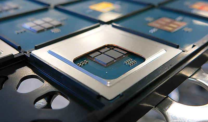
Three ways chiplets are remaking processors. AMD and Intel researchers are leaning on chiplets to boost performance, and CEA-Leti shows just how far the approach can go. The combined squeeze of rising costs and ever-larger chip sizes is leading to a solution in which processors are made of collections of smaller, less-expensive-to-produce chiplets bound together by high-bandwidth connections within a single package. The CEA-Leti processor stacks six 16-core chiplets on top of an “active interposer” made of a thin sliver of silicon to create a 96-core processor. The interposer houses voltage-regulation systems usually found on the processor. It features a network-on-chip that uses three different communication circuits to link the cores’ on-chip SRAM memories. Developers imagine a system-on-chip industry using chiplets from multiple vendors could all be integrated with standardized interfaces. (IEEC file #11715, IEEE Spectrum, 4/29/20)
Development of attachable sticker-type rechargeable batteries. Researchers at the Korea Institute of Energy Research have developed re-attachable micro-supercapacitors (MSCs) by using highly swollen laser-induced-graphene electrodes. As demands increase for smaller wearable devices and high functional IoT gadgets, there is a growing need for new technologies for power collection, storage and management. The research team successfully developed sticker-type flexible MSCs that have a flexible structure and can be attached everywhere on surfaces by using ultrashort-pulse-lasers. By impregnating adhesive polymer composites to the inside of highly swollen graphene, researchers were able to develop sticker-type MSCs with excellent electrode performance and durability, while maintaining adhesiveness. (IEEC file #11676, Printed Electronics World, 4/15/20)
Using the shadow effect to generate electricity. National University of Singapore researchers are giving shadows a positive spin by demonstrating a way to harness this optical effect to generate electricity. This novel concept opens new approaches to generate green energy under indoor lighting conditions to power electronics. The team created a device called a shadow-effect energy generator (SEG), which makes use of the contrast in illumination between lit and shadowed areas to generate electricity. The SEG comprises a set of SEG cells arranged on a flexible and transparent plastic film. Each SEG cell is a thin film of gold deposited on a silicon wafer. With careful design, the SEG can be fabricated at a lower cost compared to commercial silicon solar cells. (IEEC file #11696, Printed Electronics World, 6/4/20)
Six-junction solar cell sets two world records for efficiency. National Renewable Energy Laboratory researchers have fabricated a solar cell with an efficiency of nearly 47.1%. The six-junction solar cell now holds the world record for the highest solar conversion efficiency. This device demonstrates the extraordinary potential of multijunction solar cells. To construct the device, researchers relied on III-V materials that have a wide range of light absorption properties. Each of the cell’s six junctions are specially designed to capture light from a specific part of the solar spectrum. The device contains about 140 total layers of various III-V materials. Due to their highly efficient nature and the cost associated with making them, III-V solar cells are most often used to power satellites. (IEEC file #11677, Science Daily, 4/14/20)
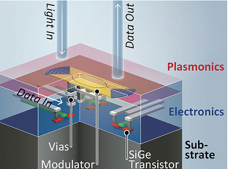
Photonics and electronics on one chip. Researchers from ETH Zurich have integrated photonics and electronics on one chip. Converting electronic signals into light signals using separate chips loses a significant amount of signal quality and limits the speed of data transmission. The integration was achieved by placing the electronic and photonic components on top of one another and connecting them through vias. This layering of the electronics and photonics shortens transmission paths and reduces losses in signal quality. As demand for bandwidth pushes datacomms above 100Gbs transmission speeds, this chip configuration provides a way forward. As plasmonic IC features are smaller than electronic ones, it now becomes possible to manufacture much more compact, monolithic chips that incorporate both a photonic and an electronic layer. (IEEC file #11799, Electronics Weekly, 7/6/20)
Scientists take steps to create a “racetrack memory,” potentially enhancing data storage. Researchers from New York University have taken steps to create a new form of digital data storage, a “racetrack memory,” which opens the possibility to both bolster computer power and lead to the creation of a smaller, faster, and more energy-efficient computer. Racetrack memory, which reconfigures magnetic fields in innovative ways, could supplant current methods of mass data storage, such as flash memory and disk drives, due to its improved density of information storage, faster operation, and lower energy use. While additional development is necessary for deployment in consumer electronics, this pioneering type of memory may soon become the next wave of mass data storage. (IEEC file #11714, Science Daily, 5/5/20)
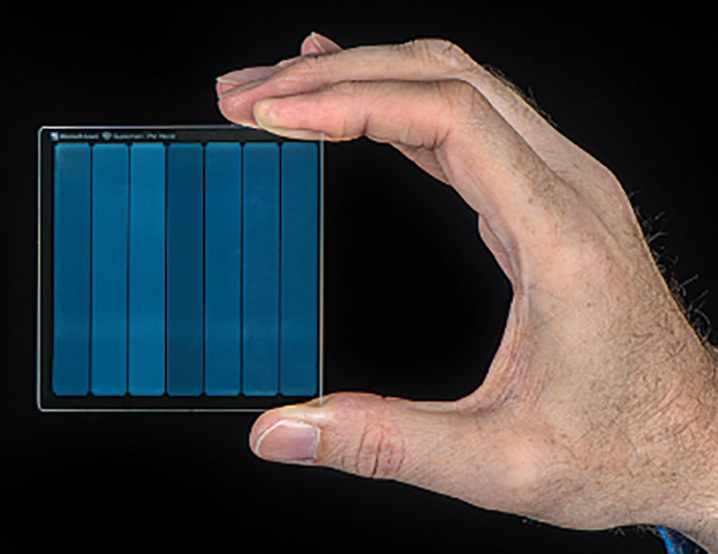
Lasers write data into glass. Magnetic tape and hard disk drives hold much of the world’s archival data. But archivists have another option: using an extremely fast laser to write data into a 2mm-thick glass where that information can remain essentially forever. Microsoft Research, in an effort called Project Silica, completed its first proof of concept by writing the 1978 film Superman on a single small piece of glass and retrieving it. Writing data to glass involves focusing a femtosecond laser on a point within the glass. The laser’s pulse deforms the glass at its focal point, forming a tiny 3-D structure called a voxel. Researchers could theoretically store up to 360Tb of data on a disc the size of a DVD. Microsoft’s work is part of a broader company initiative to improve cloud storage through optics. (IEEC file #11761, IEEE Spectrum, 5/29/20)
Crystalline “nanobrush” clears way to advanced energy and information. Oak Ridge Laboratory synthesized a tiny structure with high surface area and discovered how its unique architecture drives ions across interfaces to transport energy. Their “nanobrush” contains bristles made of alternating crystal sheets with vertically aligned interfaces and pores. The bristles of their “supercrystal,” are grown freestanding on a substrate. They synthesized the supercrystals using pulsed laser epitaxy to deposit and build up alternating layers of CeO2 and Y2O3. The achievement is proof of concept that it is possible to create vertically aligned interfaces through which electrons or ions can be transported out of the substrate's plane. Architectures like the nanobrush could be combined with other nanoscale architectures to create devices for quantum technologies and sensing, as well as energy storage. (IEEC file #11741, Science Daily, 6/8/20)
Waveguides can be laser-written into silicon carbide for photonic circuits. Optical waveguides can be fabricated in glass and other optical materials by focusing light from an ultrafast laser into the material, so a threshold peak optical power beneath the surface is reached, above which a change in refractive index occurs. In this way, the focused spot can be moved around within the optical material to create waveguides of various geometries. Shandong University researchers using a femtosecond laser have written waveguides into the bulk of silicon carbide with modal properties tailored by altering the writing parameters. The laser produced a train of 400fs polarized pulses at a repetition rate of 25Hz to write waveguides at a depth of 175µm. (IEEC file #11737, Laser Focus World, 4/19/20)
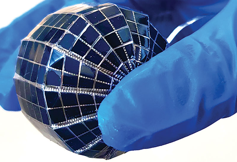
Spherical solar cells soak up scattered sunlight. Silicon solar cells folded into spheres hint at solar power's flexibility in even small devices. A new spherical solar cell design aims to boost solar power harvesting potential from nearly every angle, without requiring expensive moving parts to keep tracking the sun’s apparent movement across the sky. The spherical solar cell prototype designed by KAUST researchers is a tiny blue sphere that a person can easily hold in one hand like a ping pong ball. Indoor experiments with a solar simulator lamp have already shown it can achieve between 15% and 100% more power output compared with a flat solar cell with the same ground area, depending on the background materials reflecting sunlight into the spherical solar cell. (IEEC file #11763, IEEE Spectrum, 6/9/20)
Market Trends
Chiplets promise to help reinstate Moore’s Law and generate $5.8 billion by 2024. A new approach to semiconductor design and integration called the “chiplet” promises to help restore the microchip industry to its historic rate of advancement. The global market for processor microchips that utilize chiplets in their manufacturing is set to expand to $5.8 billion in 2024, rising by a factor of nine from $645 million in 2018. Chiplets effectively bypass Moore’s Law by replacing a single silicon die with multiple smaller die that work together in a unified packaged solution. This approach provides much more silicon to add transistors compared to a monolithic microchip. Chiplets will return to the two-year doubling cycle that has underpinned the economics of the semiconductor business. (IEEC file #11708, Semiconductor Digest, 4/28/20)
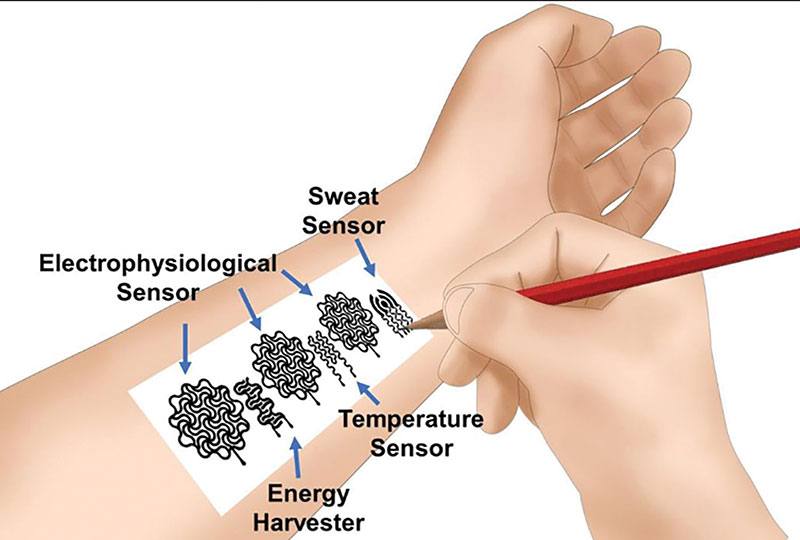
The new tattoo: Drawing electronics on skin. University of Missouri researchers demonstrated the simple combination of pencils and paper could be used to create bioelectronic devices on skin to monitor personal health. Existing commercial on-skin biomedical devices contain a biomedical tracking component and a surrounding flexible material to provide a supportive. They found pencils with 93% graphite were the best for creating a variety of on-skin bioelectronic devices drawn on commercial office copy paper. The researchers said their discovery could have broad future applications in home-based, personalized health care, education, and remote scientific research such as during the Covid-19 pandemic. (IEEC file #11827, Science Daily, 5/13/20)
Smart-labeling using battery-on-circuit technology. CPI has announced a new project to demonstrate a novel technology for printing smart “battery-on-circuit” labels that are used to track shared objects in workspaces. This low-cost power source will eliminate the need for expensive and bulky external batteries for printed electronics, overcoming a key barrier to their widening application, mass production and industry growth. The smart label can be easily attached to objects and tracked automatically through a phone app. It incorporates a key innovation that allows a battery to be inserted directly alongside the wireless tracking circuit on a thin plastic film. The low-cost battery is formed by electrochemically coating and laminating two plastic films together. (IEEC file #11728, Printed Electronics World, 5/13/20)
Biometrics market estimated to exceed $37.2 billion globally by 2024. The global biometrics market size reached $16.7 billion in 2018. Biometrics refers to a technological authentication method utilized in information assurance for secure entry, data, or access. It primarily relies on scanning physical or biological characteristics, such as the face, DNA, fingerprint, iris, retina and palm veins, which are difficult to forge or duplicate. It provides more accurate identification and lowers the risk of unwanted intrusion. As a result, biometric technologies are widely used in schools, colleges, banks, public libraries, corporate and government offices, and consumer electronics. The market value is projected to exceed $37.2 billion by 2024, expanding at a CAGR of 14%. (IEEC file #11706, Global SMT & Packaging, 4/27/20)
Recent Patents
Semiconductor device with phase-change material for thermal performance (assignee: Deere & Company), patent no. 16/167,528. A semiconductor device comprises a generally planar semiconductor chip. The semiconductor chip comprises a first side and second side opposite the first side. The first side is associated with a source conductive pad. The second side is associated with a drain conductive pad. A gate pad overlies a portion of the first side. A source terminal comprises a metallic strip assembly with a series of pocket chambers spaced apart from each other and partially filled with a phase-change material filling. A drain terminal is spaced apart from the source terminal by a dielectric layer.
Intra-semiconductor die communication via waveguide in a multi-die package (assignee: Intel Corp.), patent no. 16/643554. An interposer layer includes an integral waveguide to facilitate high-speed (e.g., greater than 80GHz) communication between semiconductor dies in a semiconductor package. An interposer layer may include a waveguide member and a dielectric layer disposed adjacent to at least a portion of an exterior perimeter of the waveguide member. The waveguide member includes a material having a first relative permittivity. The dielectric member includes a material having a second relative permittivity that is less than the first relative permittivity. The waveguide member and the dielectric member form an interposer layer having an upper and lower surface.
Printed circuit board using two-via geometry (assignee: Intel Corp.), patent no. 16/662717. To reduce the effect of undesirable electrical resonances in via stubs, a multilayer printed circuit board can electrically connect traces in different layers using two vias electrically connected to each other. For example, a first electrical trace can electrically connect to a first via at a first layer; the first via can electrically connect to a second via at the topmost layer (or the bottommost layer); and the second via can electrically connect to a second electrical trace at a second layer. Compared to a typical single-via connection scheme, the two-via connection scheme can produce stubs that are shorter in length and therefore have an increased resonant frequency that may avoid interference with electrical signals sent through the electrical traces.
Nanofluidic channel fabrication by controlled spontaneous fracturing (assignee: IBM Corp.), pub. no- US10622220. A combined nanofluidic and integrated circuit device includes a semiconductor wafer, which includes a substrate with active circuitry formed in the substrate; an oxide layer deposited adjacent the active circuitry; a stressor film deposited onto or into the oxide layer in sections, wherein the stressor film has a higher coefficient of thermal expansion than the oxide layer has, and a nanochannel formed in the oxide layer between the sections of the stressor film.
currently has research thrusts in healthcare/medical electronics; 2.5-D/3-D packaging; power electronics; cybersecure hardware/software systems; photonics; MEMS; and next-generation networks, computers and communications. The S3IP Center of Excellence is an umbrella organization at Binghamton University comprising six constituent research centers including the Integrated Electronics Engineering Center (IEEC).
is a New York Center of Advanced Technology (CAT) responsible for the advancement of electronics packaging. Its mission is to provide research into electronics packaging to enhance partners’ products, improve reliability and understand why parts fail. More information is available at binghamton.edu/ieec.


