Ensuring Reliable Products with New Rigid-Flex Design Rules
Advances in fabrication have translated into new design constraints and guidelines.
For years flex and rigid-flex typically showed up in products as a flexible cable between two rigid boards. The past five to seven years have brought tighter space constraints and miniaturization challenges. Designers must now place components on the flexible circuit, using it like a rigid substrate. Using both the rigid and the flexible areas for components, while possible, introduces new design constraints that require more advanced PCB design strategies (FIGURE 1).

Figure 1. Rigid-flex PCB designs support innovative form factors, while eliminating connectors and harnesses.
Rigid and flex PCBs often use different materials, and the rigid section usually has more layers than the flex portion. Many advanced fabricators can support these designs with more than two flex layers. To ensure flex circuits with additional layers work well in all conditions, stiffeners that bring rigidity to these PCBs are placed near components or connector areas or on the opposite side. Stiffeners are made of materials such as stainless steel or aluminum, with the addition of dielectric material like a polyimide buildup. Smaller enclosures often require the flexible portion to be bent or folded.
To prevent cracking or undue stress on components, avoid placing components and vias at the bend areas. A traditional, well-known rule is that routing must be orthogonal to the bend line to minimize material stress at the bend. Routing on the next layer through the bend area should be offset to avoid the I-beam effect. Traces that do not follow this rule may unintentionally add stiffness to an area that is intended to be flexible. Additionally, the area where rigid and flex zones come together may require overlap of material and require special spacing for holes and conductive materials. It is helpful to consider the transition zone a stress-relief area. FIGURE 2 shows a four-layer rigid board connected to a two-layer flex, which on its other side connects to another four-layer rigid board.
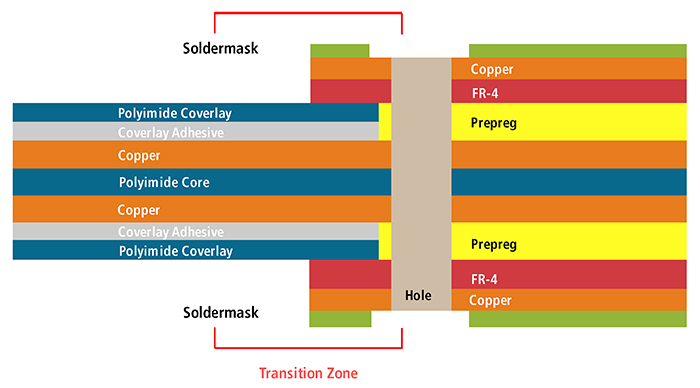
Figure 2. Sharing conductive layers between rigid and flexible substrates requires new design rules.
The PCB cross-section editor for a single stack-up must now support multiple cross-sections representing the different PCB laminates. In addition to supporting conductor, plane and dielectric layers, cross-section editors need to include new mask and coating layers above and below the surfaces of the flex PCB, such as:
- Electroless nickel electroless palladium immersion gold (ENEPIG) for special plating areas.
- Stiffeners – aluminum or stainless steel – that restrict flexing where components are mounted, to avoid cracking or peeling.
- Material masks that include (precious) metals, adhesives and solder paste masks.
- A coverlay (cover layer), which is an adhesive-coated film pressed onto the stack-up to insulate the circuit.
Advances in fabrication have extended to materials and the number of additional mask/conductive layers for flex and rigid-flex PCBs. New materials – conductive/nonconductive layers, and surface finishes – require designers to manually check if the design elements on the flex circuit are meeting the fabricator’s design guidelines. This adds a substantial amount of time to the design stage.
To avoid manual checks and ensure the design is created correctly, designers need in-design inter-layer checks to flag issues as they are created. Checking at the manufacturing sign-off stage is too late in the design cycle to find errors, and makes the design process unpredictable. Real-time capability can avoid time-consuming steps later in the process.
In-design inter-layer checks can reduce errors that may be introduced during the design process, including the following areas:
- Gap/overlap between mask layers.
- (Precious) metal-to-coverlay, mask-to-pad, coverlay-to-pad.
- Bend area/line to stiffener, component, pin and via.
- Edge-to-edge gap in areas such as the bend line to the component, via-to-bend line, and stiffener-to-bend area.
- Minimum overlap, such as when two geometries overlay by a minimum or more (e.g., solder mask overlay into the transition zone).
- Gold mask-to-coverlay, stiffener adhesive-to-stiffener, and pin-to-coverlay.

Figure 3. In this example, the display components are mounted directly on the flex circuit with a stiffener and require new design rules.
Typical Rules for Compound Designs
Mechanical constraints. Rigid-flex PCBs drive additional rules when the flex circuit is folded or bent inside an enclosure. Typically, the mechanical engineer provides the bend line, bend radius and bend area to the PCB designer. With modern EDMD (IDX) interface, this data can be automatically imported into the PCB design tools. These bend areas require designers to:
- Avoid placing vias in bend areas to avoid cracking the substrate over time.
- Avoid placing pads too close to the bend area to prevent peeling.
- Do not overlap bend areas with stiffeners, to avoid peeling.
- Do not place vias or pins too close to stiffeners, to avoid shorting.
Mechanical engineers define the boundaries for zones – rigid, flex, rigid – where the number of layers and therefore thicknesses are different in each zone. However, they need additional information about layer structures and thickness for the zones, layers above top and below bottom to accurately model the thickness of the final PCB assembly, and to perform collision checks before handing the design to manufacturing. Examples of such layers include paste mask, coverlay, stiffeners, external copper, and other materials that impact overall height, thickness, and bend performance.
Routing. Routing on flex circuitry usually requires arcs within the routes. Most of the geometry on the flex portion, including board outline, teardrops and routing, requires arcs and tapered transitions. Group routing functions must carry a group of nets (bus) across the flex, while easily locking to the contour of the flex/board outline. Transitions in line widths require tapering and all pad/via entry/exits be tear-dropped to reduce stress at the solder joints. Most PCB design tools support push-and-shove routing, but these capabilities now have to support push-and-shove with arcs in the traces. PCB designers get changes on a daily basis; adding an additional trace to a routed set of nets should not force rerouting of the entire bus.
Inter-layer checks. For advanced flex and rigid-flex designs, PCB designers need to adhere to new design guidelines from the fabricators. These new layers and surface finishes require comprehensive in-design inter-layer checks of nonconductive layers in rigid-flex PCBs. Not having these checks extends the design cycle. In-design inter-layer checks provide a correct-by-construction methodology that avoids unnecessary design iterations and, in some cases, expensive prototype builds. Tools providing a pictorial view of the stack-ups based on different substrates allow designers to visualize the layout stack-up intent as it is being defined (FIGURE 4). With an accurate picture, designers can perform more accurate DRCs, receive better feedback, and provide better data to the MCAD tool for fabrication.


Figure 4. Visualizing layout stack-up based on zones will help you avoid mistakes, like peeling stiffeners.
As there are several different materials and many new rules to adhere to, it is important to provide easy-to-understand and easy-to-specify rules for the combination of layers. A simple step-by-step process (FIGURE 5) involves:
- Choose layer/geometry to be checked.
- Choose the rule.
- Set the value.
- Select the DRC display layer.
- Add a description for the rule. (Rules must be persistent.)
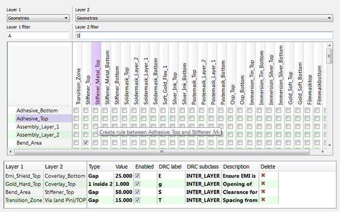
Figure 5. Rigid-flex DRCs now include new inter-layer rules specific to the new materials and multiple zones found in compound designs.
As the complexity of a flex or rigid-flex PCB increases, the amount of time a designer spends increases because of manual checks. Today’s CAD tools need to provide a way for designers to leverage new fabrication techniques without extending design time. The breadth and depth of in-design checks needs to cover 30 or more new flex and surface finish layers (TABLE 1). Users should also be able to incorporate their own layers for the tool to check, so they don’t have to wait for tool updates.
Table 1. Typical Flex Layers and Surface Finishes Used When Specifying Design Rules

is in product marketing at Cadence (cadence.com); This email address is being protected from spambots. You need JavaScript enabled to view it..


