Factors to Optimize System PIM
Laminate properties, etching quality and final finish all can affect passive intermodulation.
Passive intermodulation (PIM) has been a concern in wireless transmission systems since the 1970s. PIM affects systems that use a single antenna for both transmitting and receiving signals on multiple carrier frequencies.
Slight nonlinearities in the input/output relationship in the system can generate additional signals that are in-band at very low power levels that can increase the noise floor. Increased noise degrades system performance. Its effects are becoming more noticeable with each new generation of wireless communication technologies.
To suit a growing consumer appetite for “always-on” wireless communications, modern cellular communications technologies such as fourth generation (4G) Long Term Evolution (LTE) networks rely on advanced modulation techniques for reliable voice, video, and high-speed data communications. Such systems depend on minimal interference and low levels of PIM to function at optimum levels. Minimizing PIM usually involves evaluating the antennas in a cell site or other form of wireless base station. And low-PIM antennas start with printed circuit board laminates that can hold their own against PIM, by means of carefully selected materials, processing and advanced test techniques. With good design practices and proper understanding, control and monitoring of the PCB laminate properties, excellent system PIM can be achieved.
In a perfectly linear electrical system with multiple carrier frequencies, though “linear distortion” of power levels may occur, no additional frequencies can be generated. However, when the system exhibits nonlinearity, such as an amplifier approaching its saturation power level, additional frequencies that are linear combinations of the input carrier frequencies may be generated.
Consider two closely spaced frequencies, f1 and f2, operating in the same band (FIGURE 1). “Second-order” IM products are 2f1, 2f2, and f2 – f1. All second-order products generated are at frequencies far from the operating band, as are all even-order IM products. Third-order products include 3f1, 3f2, 2f1+f2, 2f1-f2, 2f2+f1, and 2f2-f1. While some third-order products are at frequencies far from the operating band, others (2f1-f2 and 2f2-f1) can fall in band, as shown in Figure 1. Some higher odd-order IM products (5th, 7th, 9th, etc.) may also fall in-band, though at power levels significantly lower than the third-order products.
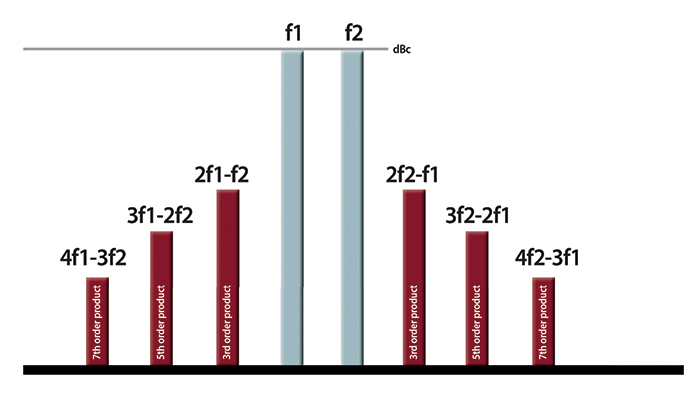
Figure 1. Passive intermodulation (PIM) is produced in passive circuits by mixing two or more carrier signals and their harmonics.
PIM is intermodulation generated in a passive system. The PIM power levels are generally very low compared to the transmitted signals that generate them. A PIM level of -153dBc indicates a power level relative to the transmitted signal of 5 x 10-16. However, since the power of the received signals is very low, PIM can increase the noise floor and lead to operational problems.
Testing for Tomorrow
A number of factors affect PIM in the transmitting side of a base station. The presence of ferrous metals or other magnetic materials in the electromagnetic field near the antenna can significantly increase PIM.
Imperfect connections, such as conductive particles or chipped plating on the mating surfaces of conductors are a frequent cause. When designing and utilizing PCB antennas, it is important to remember PIM is not a basic laminate property. Just like insertion loss, gain, directivity, and many other important electrical variables, PIM is a system property that depends highly on the system design. However, our research has determined the laminate properties that can help contribute to low PIM variables.
Antenna designers know minimizing current density is key to achieving a low PIM system.
On the laminate side, we determined high conductor purity and low conductor profile, dielectric formulation and physical properties, as well as control of the conductor-dielectric interface can be controlled properly to minimize PIM generation.
Rogers has regularly tested PIM in-house since 2002 and over that time has developed an extensive data and knowledge base. Our first PIM testing unit, a Summitek 1900b, was installed in our R&D labs and used during development and periodic materials verification. Early in 2015, we added two additional Kaelus iQA-1921c units at our manufacturing facilities producing antenna-grade materials. PIM is now routinely monitored as part of the standard production process.
The routine PIM test sample is a 305mm (12") 50Ω transmission line on 1.5mm (0.060") dielectric material in the 1900MHz band using two 43dBm (20W) tones.
Reflected PIM (also called reverse) is measured with port 1 of the sample connected to the PIM analyzer and port 2 connected to a low PIM load. Four lines are etched on a 12" x 18" laminate, and the circuit is backed by a 1.5mm FR-4 stiffener. The connection is made to the board through 0.141" solder-plated, braided low PIM cables and soldered lightweight coax to microstrip connectors. The circuits are gently manipulated, with attention to reducing the stress on the solder connection until the lowest stable PIM value is achieved and recorded. The recorded laminate value is the average of the recorded stable PIM value for each of the four lines.
When trying to differentiate between “good” PIM (perhaps in the range of -153dBc) and “great” PIM (perhaps <-160dBc), variation in the test results itself is relatively high, since it is not far from the noise floor. Thus, repeated testing is very important for developing an understanding of relative PIM. The following example demonstrates the importance in circuit design and current density in measured PIM. A 50Ω transmission line on 0.030" novel laminate typically exhibits PIM of about -153dBc. A customer routinely builds filters on this laminate that consistently exhibit PIM better than -160dBc due to the difference in current density.
For most antennas, a value of the third harmonic at -145dBc has been sufficient; although for some 3G and 4G-LTE cellular applications, a value of -153dBc or lower is required. Intermodulation effects include unwanted power diverted to other frequencies, distorted Rx signals, and low data rates and dropped calls. PIM Test Methods are addressed by the IEC TC46 WG6 – Document IEC 62037. IEC 62037 does not address testing of copper-clad laminate materials. Even so, given our testing customer input on copper profile impact to PIM, only low-profile coppers are used on antenna-grade laminates (FIGURE 2).
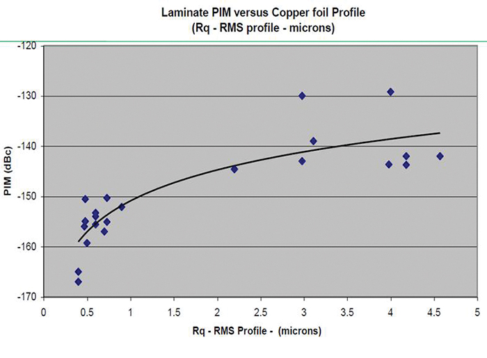
Figure 2. Relationship between copper roughness profile and PIM.
Other observations include etching residue on the surface of a circuit causes poor PIM. Etch quality also has an impact. If a circuit is under-etched and nodules of copper left in the dielectric, expect to see bad PIM. Customers have also reported ENIG results in poor PIM, whereas solder mask and immersion tin can improve PIM by up to 7dBc. PIM can result from many factors in a circuit or system, and even the thickness and dielectric constant of a laminate can affect PIM by contributing to the physical dimensions of transmission lines leading to higher current densities in densely spaced circuits.
is an associate research fellow at Rogers Corp. (rogerscorp.com); This email address is being protected from spambots. You need JavaScript enabled to view it..
Register now for PCB West, the Silicon Valley's largest trade show for the printed circuit industry, taking place Sept. 13-15 in Santa Clara: PCBWEST.COM


