Industrial CT (X-Ray) Scanning: A Substitute for Microsectioning?
Has the time come for a nondestructive test for evaluating conductors?
Recently I have been conducting empirical testing of computer simulations of trace current/temperature relationships.1,2 In comparing actual results to simulations, it is important to know the actual trace dimensions (not just the nominal design dimensions). The typical way we check the actual dimensions on a PCB is through taking a microsection of a representative section of the trace somewhere on the board. But there are some problems with microsections:
- They are destructive.
- They represent a point along a trace, but that point may not be representative of other points along the trace.
- If the actual trace under evaluation is microsectioned, the microsection precludes any follow-up testing.
- If a microsection is taken of the same place on the trace, but on another board in the production lot, this assumes the parameters of all the boards in the lot are identical, which may or may not be true.
I began thinking about the possibility of x-raying the board to see if trace parameters could be measured that way. An x-ray would be nondestructive and would allow a look at any and all points in the three-dimensional volume of the board, including the walls of vias. And it turns out there are service companies that can x-ray a board. This article explains what happened when I looked at the two alternatives for a board I was working on.
The Processes
Microsectioning. Microsectioning starts by punching out a rectangular piece from the board approximately 1" long and slightly less than 0.5" wide (FIGURE 1). The pieces are then encapsulated in a resin (FIGURE 2) and, after about 10 min. of hardening, polished (FIGURE 3). FIGURE 4 illustrates a finished microsection of a via from the board, and FIGURE 5 illustrates a microscopic close-up of the via.
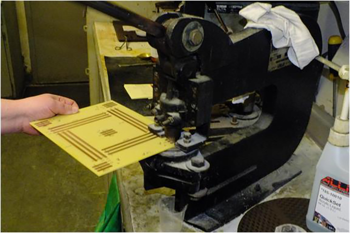
Figure 1. Punching out the microsection.
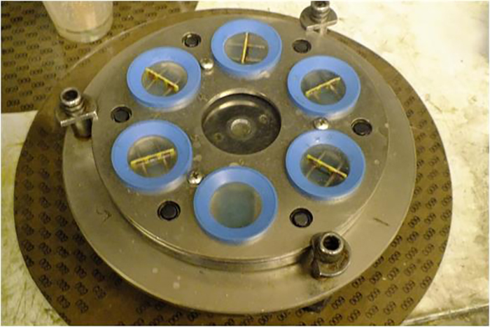
Figure 2. Microsections encapsulated in resin.
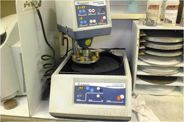
Figure 3. Polishing the microsection.
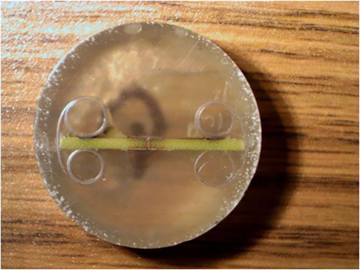
Figure 4. Finished via microsection.
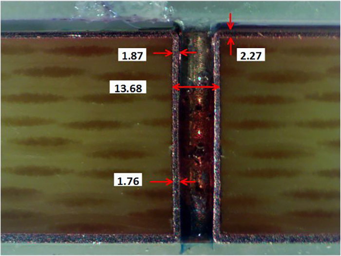
Figure 5. Enlarged view of a microsection of a via. Dimensions in mils.
It is possible to scale a view like that shown in Figure 5 and measure the dimensions very precisely (better than 0.1 mil, or 2.5µm).
The benefits of microsectioning include the ability to measure dimensions very precisely. But the weakness is that we only get a two-dimensional view of a particular 0.5 in2 cross-section perpendicular to the surface. And again, this process is destructive in its nature.
Industrial CT scanning. Industrial CT scanning (also sometimes called computed tomography)3 is somewhat similar to a medical CAT scan. Referring to FIGURE 6, an x-ray source sends out a beam in a roughly conical shape. The target (think PCB) is placed in the path of the beam. A sensor collects the beam and generates a digital representation of the target. The closer the target is to the source, the larger the magnification will be. But, the closer the target is to the source, the smaller the area of the target that can be analyzed.
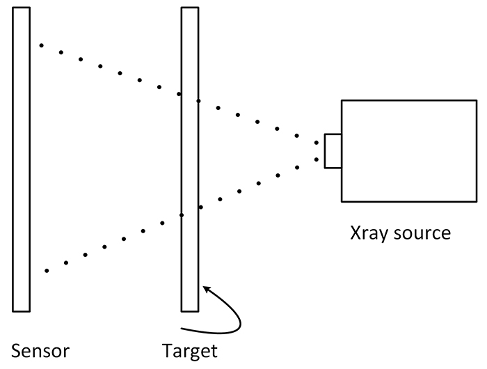
Figure 6. X-ray process.
The target is rotated 360°. Individual x-rays are taken as the target rotates. Roughly 2,200 x-rays are taken during a 360° rotation! The magic happens when the software collects all those digital images and combines them into a data file that can be viewed as a 3-D image (with a special software viewer). FIGURE 7 illustrates the actual equipment used for generating the x-rays for this project.
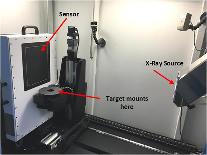
Figure 7. X-ray equipment used for this project (courtesy Jesse Garant Metrology Center).
The view that got me excited about computed tomography is shown in FIGURE 8. This is from one of the libraries at Jesse Garant Metrology Center. What is readily apparent is a trace is missing at one of the pins on one of the inner layers. (The desire to locate the exact point of this failure was one of the reasons this particular board was x-rayed in the first place.) It is possible, by adjusting the depth of this image, to actually look inside the IC packages mounted on top of the board.
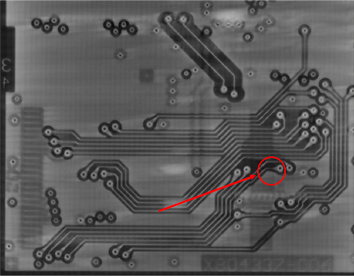
Figure 8. View of an innerlayer of a board. Note the failure at the point indicated by arrow.
Results
FIGURE 9 shows my particular test board. The viewer is positioned at a point with a via exactly like the via shown in Figure 5. The bottom right image is that of the board. (It was cut to fit on the target stand. More about that later.) The other three quadrants provide views in the three primary axes. The upper right quadrant is viewing down onto an x-y plane at a particular point along the z-axis (y is up; x is to the right; z is into the page). In this view, the plane is the middle of the trace slicing through the via. The line points to the via. The upper left quadrant is the view looking back in the y-direction at a point along a plane in the x-axis (y is up; z is to the right; x is into the page). The line points to the same spot on the via. The lower left quadrant is looking from left to right on the x-axis along the plane in the y-axis (x is up; z is to the right). Again, the line is pointing to the same spot on the via.
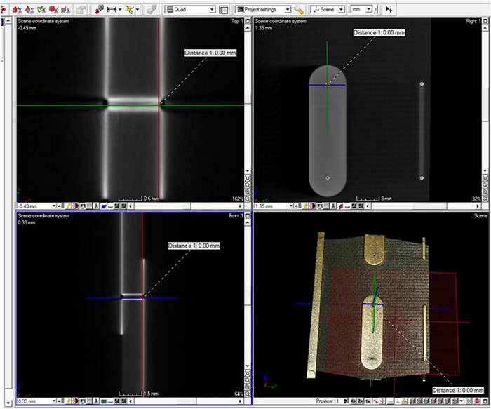
Figure 9. X-ray images of my board.
The image point can be moved to any arbitrary point in 3-D space and can be zoomed in or out to reveal any desired area. One of the many tools available in the viewer is the precise measurement between any two points in the board. Unfortunately, the resolution in this image is not quite sharp enough to measure the via width or the thickness of the copper plating.
Two aspects of this ability are particularly intriguing:
- I can look at any point inside any and all vias.
- I can examine the entire length of any trace in all three dimensions.
But the problem? The resolution is not quite good enough to take measurements with the required accuracy. The process is excellent for qualitatively analyzing the makeup of the board (including the interior of any components that might be mounted on the board), but not quite suitable for quantitatively measuring the trace parameters. So we can tell if a trace is missing, or if there is a marked difference in the plating thickness on opposite walls of a via. Within reason, we can locate opens and shorts (except possibly hairline shorts). We can evaluate if there are significant non-uniformities in the plating along a trace. We can even evaluate some solder problems. But we can’t precisely measure any of those anomalies.
Can the resolution be improved? Perhaps. If the target is moved closer to the x-ray source, then the image is larger, and more precise measurements are possible. But a smaller area of the total board is then visible. Here are some possible advances:
- Increase the power at the source (along with some attendant power management and cost issues).
- Shorten the wavelength of the source.
- Increase the sensitivity of the sensor.
All these are potential solutions, but are not practical today. We can anticipate they might become practical at some point in the future.
Comparison of Processes
As mentioned several times, the microsection process is localized and destructive. The industrial CT scanning (potentially) allows coverage of the entire board and is not destructive. The x-ray process can be used after components have been mounted on the board; the microsection process, probably not.
The resolution for the microsection process is suitable for quantitative analysis; for x-ray, we can really only do qualitative analyses.
The physical board size may be an issue. We can microsection a piece out of virtually any board, regardless of size. A limitation, however, on the size of the board can be placed on the platform for x-ray analysis. Today that size is approximately a 5" or 6" square, depending on what exactly we want to do. From a practical standpoint there is no thickness limitation for either approach.
The microsection process is very low cost, requires relatively little capital equipment, and can be performed by a fabricator. The x-ray process, on the other hand, requires a large capital investment and requires time for access and processing of the image. It is only practical at companies specifically equipped to provide the service. These comparisons are summarized in TABLE 1.
Table 1. Comparison of the 2 Approaches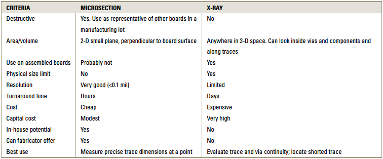
There are several benefits the industrial CT scanning process offers us in the PCB industry today. And, it was very interesting looking into it. It is suitable for troubleshooting the continuity of traces and probably for evaluating the uniformity of the plating of traces and vias. It would almost certainly allow discovery of a precise point of a conductor short circuit inside a board. Unfortunately, the primary benefit I was hoping to achieve (quantitatively measuring the trace) is not practical – yet! But I have hope for the future.
References
- Douglas G. Brooks, Ph.D., “Empirical Results of Fusing Tests,” PCD&F, January 2016.
- Douglas G. Brooks, Ph.D., “Empirical Confirmation of Via Temperatures,” PCD&F, February 2016.
- There are some significant differences between industrial CT scanning and a CAT scan. The output of industrial CT scanning is a data file that allows the user to look anywhere in 3-D space. The output of a CAT scan is typically one or more 2-D views of the area of interest in the patient. A simple medical x-ray of a patient produces a single picture. Single x-rays of an industrial product are referred to as industrial radiography. Industrial radiography and industrial CT scanning can be done at much higher power levels than can be done in medical, which means they can scan denser materials with higher resolution than is available in medical imaging.
Acknowledgments
This type of study would not have been possible without the generous support of a lot of people. My ex-partner, Dave Graves (now with Monsoon Solutions in Bellevue, WA), was very helpful in finalizing some board designs. Prototron Circuits (Redmond, WA, and Tucson, AZ) was very helpful in providing test boards. They also provided microsectioning services, including allowing me to photograph the process. Fabio Visentin and Alejandro Golob of Jesse Garant Metrology Center, Windsor, Ontario, provided x-rays of the board and showed me how to analyze those x-rays. Nathaniel Peters of W. M. Keck Center for Advanced Studies in Neural Signaling provided valuable support in microscopy.
, is owner of UltraCAD Design, a PCB design service bureau and author of PCB Currents: How They Flow, How They React; This email address is being protected from spambots. You need JavaScript enabled to view it..


