How Should You Mark Your Diodes?

Steps to avoiding ambiguity when identifying current flow.
Current flows through a diode from the anode to the cathode; it will pass current only when the potential on the anode is greater than the potential on the cathode. This is mostly true, but not always.
For the common barrier diode, or rectifier, it’s a pretty safe bet. However, with a zener diode, or TVS, it’s not true. And that is why marking a diode on the printed circuit board with the plus sign (+) is not good practice.
Look at the schematic in FIGURE 1. Once this circuit is put on a PCB, a plus sign could be legitimately placed on the anodes of D3 and D4, and another on their cathodes. In FIGURE 2, a designer could legitimately place both a plus sign and a minus sign on the anode of D9. In both of those cases, the marking would be technically correct, but would not convey the whole story.
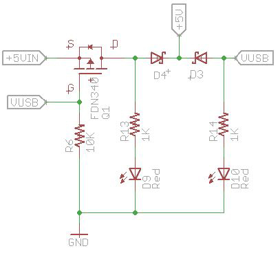
Figure 1. In this circuit, a plus sign could be placed on the anodes of D3 and D4, and another on their cathodes.
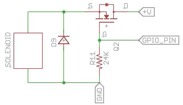
Figure 2. In this circuit, both a plus sign and a minus sign could be placed on the anode of D9.
As an assembler, we won’t necessarily know what the designer has in mind, and we don’t have the schematic. If you use the practice of marking diodes with a (+) on the anode, we don’t have any more information than if you didn’t mark it at all. The same holds for using a minus (-) sign. It really doesn’t give us any information.
How should you mark your diodes? The best method is to put the diode symbol next to the footprint on the board. You can also use “K” to indicate the cathode and “A” to indicate the anode. “K” is used because “C” could be mistaken for “capacitor.”
D5, in FIGURE 3, would be the preferred method. D7 will work as well. If there is not enough room on the board due to space constraints, you could put the same information in an assembly drawing.
Ambiguity is the enemy of manufacturers everywhere.
is marketing manager at Screaming Circuits (screamingcircuits.com); This email address is being protected from spambots. You need JavaScript enabled to view it..
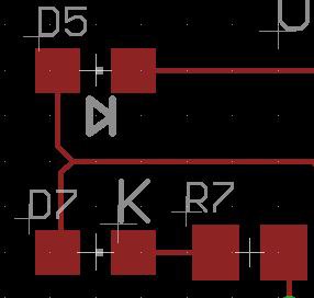
Figure 3. The best method is to put the diode symbol next to the footprint on the PCB.


