Don’t Let Your Signals Stub Their Toes
Via stubs can be tamed by keeping the length short, restricting signal layer transitions, and utilizing back drilling in multigigabit applications.
You need to read this article because you’ve built your backplane
with the lowest dielectric loss laminate you could afford. The
connectors are rated at 20 GHz bandwidth, and your trace impedances are
within 5% of 100 Ohms. Your SERDES I/O drivers have multi-tap
de-emphasis and equalization built in. All 50 inches of path length is
perfectly matched and tuned. You’ve simulated the system with a pretty
good link analyzer and have confidence you will see a 10 Gbps eye that
is open with plenty of margin over the eye mask.
But,
when you power on and look at the eye for the first time, it’s nearly
closed. The bit error rate (BER) is 0.1%, more than nine orders of
magnitude higher than you expected! So, what went wrong? What’s killing
the signal?
Like a tiny clot in an artery that can
take a person down, one of the killers of high speed serial links is
the via stub, a tiny piece of interconnect, that can take down a
backplane many times its size. It is an artifact of the process of
manufacturing through hole vias, and can be the death of a high speed
interconnect.
Through Hole Vias
Vias
are essential structures in all multilayer circuit boards that enable a
signal to switch from one layer to another. The through hole via –
often referred to as a plated through hole (PTH) via – is by far the
most common and the lowest cost via in multi layer boards. After the
entire board is laminated in a press, vias are mechanically drilled
through the entire stack, and the inside of the hole (called the
barrel) is metallized to make it conductive using an electrochemical
plating process. Surface traces and pads are plated at the same time.
Every
through hole is capable of connecting any layer to any other layer.
Each through hole is programmed by the pads, signal lines or planes
that intersect the drilled hole. When a drill passes through copper on
any layer, the edge of the copper inside the hole is exposed, and when
the entire barrel is metallized, any exposed metal is electrically
connected.
In a multilayer board, a via may connect a signal from any layer to any other layer. In the case of the 12-layer board shown in Figure 1, the via connects signal layers 1 to 4.
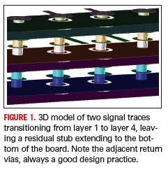
As
part of the manufacturing process, the via is plated all the way
through the board, even though the signal itself may only travel
through part of the barrel. The rest of the barrel (in this case, below
layer 4) is called the stub. The residual stub acts as a short
transmission line to the signal. At low frequency, the impact is a
capacitive load, but at high frequency, it is a resonant structure that
can have a dramatic impact on signal integrity.
Electrical Performance of Vias
The
only way to know the precise electrical performance of the stub is by
either simulating the via performance using a full wave electromagnetic
simulation tool, or building a test structure and measuring it.
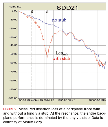
Figure 2
shows the measured insertion loss of a long backplane trace with a
signal layer transitioning from the top layer to layer second from the
top, with a resulting residual stub of about 200 mils long.
Of
course, changing any of the geometry features, such as clearance holes,
location of return vias, plane-to-plane spacing and even barrel
diameter, will change the performance.
In the absence
of a measurement or a full wave 3D simulation for every via, we can get
a very good estimate of the electrical impact of a via, and identify
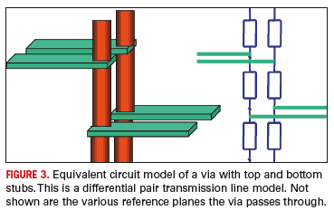
the main features that affect its performance, by modeling it. The
modeling should combine simple, uniform, single ended or differential
transmission lines that are evaluated for performance using a SPICE
simulation tool. An example of the circuit topology of a differential
via is shown in Figure 3.
There
are only two parameters that define a single ended transmission line;
its characteristic impedance and its time delay. For a differential
via, you must include both its odd and even mode impedances as well as
the time delay.
What is the characteristic impedance
of a via barrel, with its return path being a combination of adjacent
return via and coupling to the planes it passes through? The answer is
the most common answer offered in signal integrity, “it depends” – on
the barrel diameter, clearance hole size, presence of non-functional
pads, and spacing between the planes. However, for most typical design
rules, the via impedance will range from 30 to 70 ohms. Given its short
length, typically less than 200 mils, even this wide range of impedance
has only a small impact on a signal.
The signal
degradation introduced at a via is not from the via barrel path, but
from the stubs connected to the ends of the via barrel. Add a 30-Ohm
stub that is 200 mils long to a short via and the insertion loss can
drop by more than 30 dB, dramatically affecting transmitted signal
quality. Figure 4 compares the simulated insertion
loss of a 200 mil long, 30 ohm via with no stubs, to a short via (from
layer 1 to layer 4) with a 200 mil long via stub.
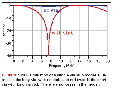
There
is a huge resonant dip at the frequency where the length of the stub is
one quarter of a wavelength. Any frequency components of a signal near
this resonant frequency will be completely blocked by the via stub.
Stub Length and Resonant Frequency
The
high frequency behavior of a via is dominated by the interference
caused by the transmitted signal, along with the signal that reflects
off the bottom of the stub. This is illustrated in Figure 5.
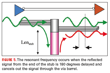
The
signal incident to the via is traveling down the 50 ohm impedance of
the top signal line. The signal enters the via and hits the ‘T’
intersection where the signal splits. About half the signal travels
down to the second signal layer, following in the wake of the initial
signal heading to the receiver.
The two signals
traveling in the forward direction to the receiver will interact with
each other. If the extra path length the signal took in going down the
via stub, reflecting and coming back up the via stub (a round trip
delay) is half a cycle, then the two signals traveling to the receiver
will be out of phase and they will subtract.
The
frequency where this first resonance occurs is when the round trip
delay of the stub is half a cycle. This corresponds to a resonant
frequency of f = 1.5/Len, with the frequency in GHz and the via stub
length in inches.
If the resonant absorption from the
via is to have little impact on the transmitted signal, then its
resonant frequency must be much higher than the bandwidth of the signal
in the data stream. The bandwidth of the signal is the Nyquist
frequency, which is roughly one-half times the bit rate. For the via
stub to have no affect on the transmitted signal, the resonant
frequency of the stub should be much higher than the signal bandwidth.
As
a rough rule of thumb, if BR equals the bit rate in Gbps, this means f
> ~ 10 x ½ x BR, or via stub length, in mils < 300/BR. A 10 Gbps
data stream should have all stubs of less than about 30 mils in its
signal path.
Optimizing Stubs
The
first step in minimizing the impact from stubs is to keep their length
as short as possible. In a multilayer board, one way of keeping stub
lengths short is by limiting the signal layer transitions. In an
extreme case, high-speed signals will only be routed on the top and
bottom layers so that any via between these layers will have no stub at
all.
A slight amendment to this design guideline
might be to limit any high-speed signal transitions from near a top
layer to near a bottom layer. This will limit the length of a via from
the surface to the lowest signal layer. For example, never route a
signal from layer 1 to layer 4, but you can route a signal from layers
1 through 4 to layers 10 through 14.
If you can’t
make a via stub shorter, then the next knob to tweak is to increase
their impedance by decreasing their capacitance. This can be
accomplished by:
- Use as narrow a barrel diameter as possible
- Minimize the size of capture pads on the top and bottom surfaces
- Remove all non functional pads on all intermediate layers
- Increase the clearance holes through all planes as much as possible
Every
decrease in capacitance will help reduce the impact of the via stub.
How do you know if it is enough? Use a full wave 3D field solver to
simulate the via and its stub, or build a candidate via in a test
coupon and measure it.
Back Drilling Stubs
Sometimes
it is not possible to restrict the layer transitions, and no matter how
low you get the capacitance, you still have a stub and the impact of
its resonance. You might still be able to eliminate the via stub by
using blind or buried vias. An alternative is to back drill the via
stub to remove the conductive barrel.
Back drilling
has become a conventional process that most fab shops routinely do with
only a small price premium. The through hole via is manufactured in the
conventional way, and then a drill bit with a diameter a few mils
larger than the barrel is used to drill out the stub from one side of
the board. This requires controlled depth drilling, which can typically
be controlled to within 5-10 mils.
Using back
drilling, residual via stubs can easily be kept to less than 20 mils,
which enables good signal quality for even 15 Gbps signals. Many
backplanes have demonstrated more than 10 Gbps operation with
conventional FR-4, pre-emphasis and equalization and with back drilled
vias.
Conclusions
A tiny via stub, less than 150 mils long, can affect the performance of a high-speed serial link much more than an entire 50 inch long interconnect. The stub can be tamed by keeping its length short. Using the combination of careful design guidelines in the physical design of a via and restricting signal layer transitions, along with technology options such as back drilled vias, a high-speed designer should not hesitate to incorporate vias in multigigabit designs. PCD&F
Dr. Eric Bogatin is president of Bogatin Enterprises LLC; This email address is being protected from spambots. You need JavaScript enabled to view it..


