Plating Voids, Parts 1 and 2

The objective of metallization is deposition of a continuous copper layer.
The German author Kurt Tucholski defined a hole as the following:
1. “A hole is where nothing exists.”
2. “ A hole is a permanent companion of the non-hole.”
3. “ If man sees a hole, he intends to fill it. While doing so, he often falls into it.”
Certainly,
the objective of the metalization operation is to put something into
the holes, namely a continuous, void-free and tightly adherent deposit
of copper. However, despite good intentions, one does not always
accomplish this. The result is voiding: those areas on the resin or
glass or at times both that do not receive the copper deposit.
Mention
the word “voids” in a PCB facility, and watch everyone scramble. The
problem with voids in plated through holes (PTH) is that there are so
many potential causes that it is very difficult to quickly identify the
source or sources of the problem. It is the purpose of this and the
next few columns to discuss voiding and its causes in detail.
Generally,
voiding is most often blamed on the metalization process itself.
Certainly, this process is not without blame. However, since PTH
metalization and the desmear process are so interdependent on each
other, it is easy to see that the upstream processes can influence a
defect that manifests itself later in the sequence. We will discuss
this in detail later.
The IPC-A-600 standard provides an excellent guideline with respect
to voids. Basically, if your company is building PCBs for Class 3, any
voiding is considered a nonconforming defect. This includes glass
voids, resin voids, circumferential voids ... any voids. Voids come in
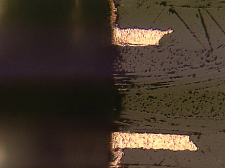
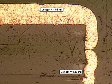
all shapes and sizes. Some are very evident, such as the one seen in FIGURE 1. Other voids are much more subtle, as shown in FIGURE 2. Basically, we strive for a continuous void-free deposit as shown in FIGURE 3.
|
|
|
|
|
|
Assume voiding has been discovered. An analysis of the problem tells
you that the voiding is confined to the glass only. The resin coverage
looks fine. Backlight testing confirms voiding through the electroless
copper process. The voids are on multilayer PCBs made with a
tetrafunctional resin. This resin system is used regularly in the PCB
facility, so there are no new wrinkles here. Where would the
troubleshooting effort start? Let’s first discuss the possible causes
of glass voiding.
Numerous possible causes for glass voiding are listed below:
- Insufficient cleaning and conditioning of the holes
- Drill debris in holes
- Overall poor hole wall quality
- Insufficient or ineffective desmear
- Permanganate or manganate residues remaining on resin
- Insufficient catalyzation (in electroless copper preplate)
- Insufficient acceleration (leaving excess tin and not allowing palladium to initiate the deposition reaction)
- Air/gas bubbles lodging in small diameter vias
- Inadequate rinsing
- Panels racked too close together
- Rack agitation.
These are just a few of the causes of voids. One of the first places
to look is the cleaner/conditioner step. This step is critical to the
success of the electroless copper process in that the conditioner
enhances the adsorption of the activator species (palladium) to both
the resin and glass.
Inadequate conditioning will reduce the charge density on the glass
and resin, resulting in less than optimal palladium (activator
adsorption). This condition will lead to lack of a continuous void-free
copper deposit in the hole. Sufficient activator is necessary to
catalyze the electroless copper reaction.
Essentially,
the cleaner/conditioner can be described as an activator promoter.
After all the examinations are complete and the problem is minor glass
voiding, (no evidence of resin voids), then the first place to look is
the cleaner/conditioner. Generally, the concentration of the
cleaner/conditioner or the operating temperature is less than
recommended by the process supplier.
Another cause is that the useful life of the made-up solution has
been exceeded. In this case, the “spent” chemistry must be sent to
waste treatment, and a new solution made ready. If this doesn’t solve
the problem, there are other areas to look at.
Pre-Electroless Causes of Voids
|
|
It is often said by seasoned engineers that there are so many
process steps and variables that could have an influence on the success
or failure of getting a continuous, void-free copper deposit in the
hole. One of the obvious causes of voids or at least poor copper
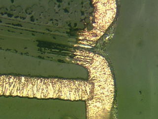
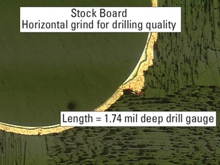
coverage is the result of poor drilling. Figure 4 shows voids
on the glass bundle fibers. A closer look as this section will show a
very poorly drilled hole wall, with glass bundles protruding from the
resin.
Astonishingly, many feel the plating process should always
compensate for such a travesty. A surface such as the one shown in
Figure 4 makes it very difficult to catalyze with the palladium-based
activator from the electroless copper process. One should immediately
investigate the drilling operation, looking at the following:
- Drill bit quality: the number of hits and the overall condition of the drill tool.
- Spindle feeds and speeds: is the drill tool punching its way through the stack?
- Slow up-feed – causing the torn out glass bundles – should be 2X the in-feed rate.
- Check chip loads: experiment with different chip loads to improve quality.
- Stack height: the number of PCBs in the drill stack; consider reducing the number to improve quality.
Figure 5 shows a horizontal section of a PTH. Note again the poor quality in the hole wall and its effect on the plating process.
|
|
The desmear operation is another potential cause of PTH voids. The
most effective desmear process available today is based on alkaline
permanganate. As a matter of fact, the permanganate system is
considered an industry standard. The use of alkaline permanganate for
multiplayer PCBs has had a dramatic effect on copper coverage and
adhesion in the plated through hole. However, this process, if not
controlled, can be a major cause of voids. First, the process consists
of three or four steps, as listed below that comprise the main chemical
process for desmear.
1. A solvent conditioner designed to penetrate the polymer matrix of
the resin system and weaken the polymer-polymer bonds of the cross
linked chain.
2. The alkaline permanganate solution consisting of sodium or potassium permanganate and its corresponding hydroxide salt.
3. A neutralizer (possibly in combination with glass etch) for removing manganese residues.
4. Glass etch as a separate step to lightly roughen (frost) or more
aggressively remove glass fibers that may be protruding into the hole
due to etch back.
Any of these four processes if not controlled can lead to voids. If
this is the case, even the most robust of electroless copper processes
will not be able to compensate.
|
|
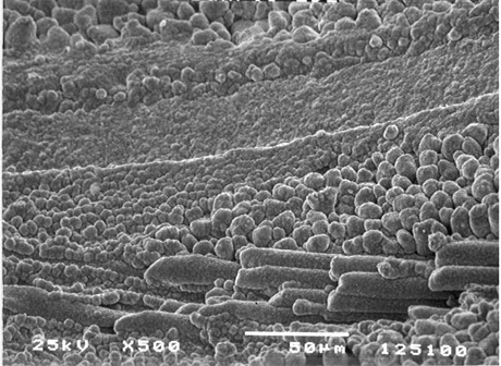
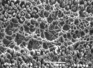
For example, the effective alkaline permanganate process not only
removes drill smear, but will micro-roughen the resin as shown in Figure 6. This texturing is often referred to as the honeycombed appearance. This is desirable for two reasons:
- The textured surface promotes palladium catalyst adsorption, which in turn promotes electroless copper deposition and coverage.
- Surface improves copper adhesion.
This, in turn, promotes improved solderability by minimizing or
eliminating the occurrence of blow holes seen in the wave-soldering
operation. More on blow holes in a future column.
Regardless, if the texturing is inadequate, the possibility of voids
exists. The main reason is that the lack of texturing will reduce
catalyst adsorption, leading to voids. Electroless copper processes
require an adequate amount of catalyst on the hole wall to promote the
electroless copper deposition. Key questions to ask in the
brainstorming session include the following.
- Is the solvent conditioner (swellant) making sufficient
penetration into the resin matrix? And is the solvent system compatible
with the resin that you are trying to desmear? It should be noted here
that some of the higher Tg resins do not react in the same manner as
standard FR-4 and require specialized solvent conditioning. The higher
the degree of cross-linking in the polymer resin makes the more
difficult it is for the solvent to penetrate and, thus, weaken the
polymer-polymer bonds in the resin. In turn, this reduces the action of
the permanganate solution in terms of resin removal and
texturing.
- Check the operating temperature of the alkaline permanganate solution, as well as the hydroxide and actual permanganate content. The hydroxide content aids in promoting the aggressiveness of the permanganate attack on the resin. The permanganate in the +7 oxidation state will perform the actual oxidization and breakdown of the resin. Manganate (+4) is a by-product of this reaction and will not participate in the resin oxidation. Manganate residue should be controlled and maintained below 20 to 25 grams/liter. Otherwise, as manganate builds up over time, the rate of resin removal and texturing will diminish. If solvent compatibility and degree of penetration is sufficient, then consider utilizing a higher concentration of permanganate. Sodium permanganate will allow for more actual permanganate in solution over the corresponding potassium salt.
- Finally, review the neutralizer and glass-etch. A major cause of
voiding is due to manganate residues remaining on the hole wall resin
and glass. One should frequently renew this solution to ensure fresh
working chemistry. Also, check the acid concentration. Lower
concentration reduces the effectiveness of the neutralization.
Often, to reduce process steps, fabricators will combine the
neutralizer and glass etch in the same process tank. (Personally, I
prefer separate steps because the process is more effective.) As the
glass etch weakens due to continued use, the ability of the glass etch
to roughen the glass fibers (referred to as “frosting”) is reduced.
This, in turn, reduces the ability of the catalyst to adhere to glass.
When this happens, voids can result. PCD&F
Michael Carano is vice president, marketing and business development at Electrochemicals Inc. He can be reached at This email address is being protected from spambots. You need JavaScript enabled to view it..
