Copper Via Fill – A Solution for HDI Via-in-Pad
Via fill for via-in-pad designs improves manufacturability from board fab through assembly.
High density interconnect (HDI) and microvia technology have been
commercially available for years, but many sectors of the electronics
design and manufacturing community have historically regarded these as
alternatives that should not be pursued until absolutely necessary.
Concerns with higher complexity design processes, expensive performance
qualification tests and lower assembly yields have hindered the
adoption due to fears of increased product costs.
While
all these factors generally apply to any new technology, they also
usually get worked out as the technology matures. The mass production
of portable electronic products such as mobile phones, personal digital
assistants (PDAs) and music players--all of which we could not enjoy
without this enabling technology--have provided ample opportunities for
the relevant issues to surface and be addressed. Yet, some technology
sectors are still reluctant to adopt HDI. Ironically, we communicate
our concerns about HDI technology over devices that employ it.
Microvias, as indicated by their name, are very small vias, usually
ranging from less than 6 mils or 150 microns in diameter down to 2 mils
(50 microns) or less. They are typically located near the centers of
the PCB pads and can be seen under magnification as small dimples or
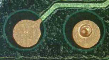
depressions in the pad. Figure 1 shows a 10-mil pad with a 4-mil microvia.
|
|
The past four or five years have seen the emergence of many more
devices that require the use of microvias in all types of applications,
even those demanding long-term reliability performance. In some cases,
they are impossible to avoid, as the desired semiconductor chips are
only available in packages that require microvia-in-pad technology on
the PCB. In other cases, such as advanced aerospace applications,
package size and weight cannot be increased, despite the ongoing need
for improved electronic processing performance. The point of acceptance
for the technology step is eventually reached and crossed.
Embracing HDI and microvia technology can bring many benefits, the most
notable of which include significant reductions in layer count, smaller
circuit areas, higher component counts, thinner boards, shorter design
times and, ultimately, less expensive material constructions. But there
is no such thing as a free lunch, and such gains do not come without
some real technology challenges to both the fabricator and the
assembler. Historically, microvia-in-pad designs have presented plating
difficulties to fabricators and soldering difficulties to assemblers.
On the plating front, using conventional PCB fabrication processes and
equipment, a blind microvia size of 2 mils (50 microns) or even 4 mils
(100 microns) can present significant challenges with regard to
wetting, plating and other processing. The following types of defects
have been known to result:
- Breakdown in the continuity of the base copper metallization (voids)
- Incomplete coverage of the final surface finish due to contamination
- Voiding due to etch out of the electroplated copper as a result of incomplete or porous electrolytic tin-etch resist coverage
- Entrapped corrosive process chemistries resulting from poor rinsing and drying
On the assembly side, microvias present a separate set of
challenges. It has been documented that in the case of small discretes
like 0402s or 0201s, the parts can rob solder from the joint being
formed, raising reliability concerns. The bigger concern, however, is
the issue of voiding when microvias are in the pads of area array
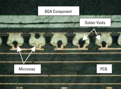
devices, such as microBGA-style components. Figure 2
shows a cross section of an area array device with microvias in every
pad. Considerable voiding is observed in these joints. These large
voids occur because the depression in the pad surface traps air during
the solder paste printing portion of the assembly process.
|
|
The correlation of void size to the reliability of BGAs is a
long-standing point of contention in the assembly community. Most
assemblers avoid the debate but subscribe to the position that the
smaller and fewer the voids, the better. A print-reflow process that
runs typical maximum void size rates in the neighborhood of 5% can see
that number soar to 25% and higher when microvias are introduced. From
this, only about 5% can be attributed to the solder paste, with the
remaining 20% coming from the microvia itself. These numbers can alarm
any engineer associated with the success of the product under
consideration, regardless of his or her general position on void size
and reliability! To make matters worse, the leakage of entrapped
moisture or residual contaminants in these relatively inaccessible
blind via-holes during or after the fabrication process can provide
additional contributions to void formation.
The voiding issues encountered at board-level assembly are
nondiscriminatory with respect to the final solderable finish of the
PCB. They manifest themselves on all of them, but not always in the
same exact way. The low rate of spread of lead-free solders on copper
OSP finishes result in a void that does not move within the solder
joint; the trapped air stays in its original location within the
microvia. The higher rates of spread of the same solder alloy on ENIG
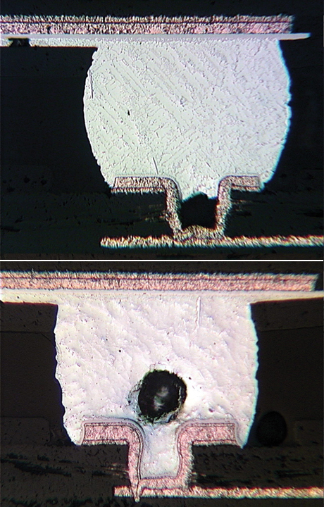
finish helps to liberate the trapped air into the bulk of the joint. Figure 3
shows two similar 0.5-mm pitch CABGA (Chip Array Ball Grid Array)
solder joints with unfilled 4-mil vias in their pads. The one on the
left has an OSP final finish; the one on the right has an ENIG final
finish. The debate regarding the optimum location of the void within
the joint continues, but the general opinion leans toward containing it
within the via, as seen on the OSP finish.
|
|
The bad news here is that microvias in pads help to produce very
large voids in very small solder joints. The good news in this case is
that there are relatively simple solutions at hand. A range of
via-filling technologies is available to the fabricator. These include:
- Inorganic thick-film pastes
- Organic pastes including unfilled, metal filled and inorganic filled types
- Electrolytic copper plated via-fill
All
these via-fill methods can improve structural integrity and provide
varying degrees of enhanced thermal relief. However, whereas the
processes that use pastes are typically suited to larger through-hole
vias (>10 mils or 0.25 mm diameter), processes that use plated
copper are more suitable options for smaller, blind microvias (<7
mils or <175 microns diameter).
The copper
filling of vias can benefit design performance by improving thermal
conductivity, providing a known CTE compatibility with the board
metallization and readily supporting “stacked via” designs. But the
benefits don’t end there. For the fabricator, some of the available
copper via fill processes offer simultaneous conformal plating of the
through holes while achieving complete filling of the microvias, thus
eliminating the unwanted, additional process steps associated with
paste filling processes. And for the assembler, if the pads do not have
the small, deep air-trapping wells on their surface, the issue of
excessive voiding is practically eliminated.
There
is a further advantage here for the fabricator. The technology that
plates through holes while simultaneously filling blind microvias is a
simple one that drops into existing vertical electrolytic plating lines
using soluble copper anodes. The concept and application are described
as follows.
Simple Copper Via Fill Process
Electrolytic
copper baths that are based on a sulfuric acid and copper sulfate
typically contain “brightener” or additive systems, which incorporate
an activator and a suppressor, plus other components. Such single-step
processes are typically more difficult to control, as the analysis
involves more complex CVS (cyclic voltammetric stripping) techniques to
measure the multiple components. However, the copper process utilized
in this study does not contain any activator in the electrolytic step.
Instead, the proprietary1
process actually works on a simple two-step system where the PCBs are
first pre-dipped in an activator bath before transferring to the
plating cell that contains the suppressor. At start-up of the plating
cycle, the adsorbed activator from the pre-dip is already concentrated
in the lower current density areas, i.e. within the blind microvia
recesses. As plating progresses, the larger and slower moving
suppressor molecules restrict any excessive and unwanted copper
deposition on the panel outer-surfaces, which results in fast and
efficient filling of the microvias. The use of the two separate baths
make CVS control much more precise.
Additionally, the
total organic levels in the plating bath are moderated, therefore
improving the physical integrity of the copper deposit and its
resistance to cracking under thermal shock conditions. The copper
deposited by this process meets and exceeds all the standard deposit
performance test requirements for through-hole metallization, showing
typical elongation values of 28% and tensile strengths of 44,000 psi
(304 N/mm2). These values are well in excess of IPC-6012B minimums, which are cited as 12% elongation and 36,000 psi (248 N/mm2).2
This simple two-step process is operated in a standard, vertical DC,
air-agitated plating cell, thereby eliminating the need for any
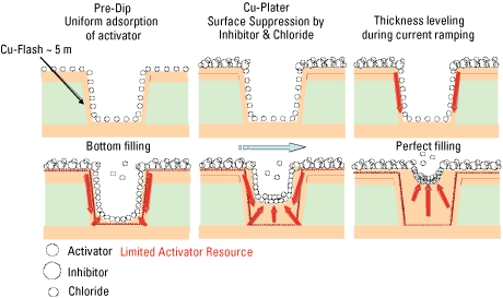
specialized equipment3. A schematic diagram of the via-filling mechanism is shown in Figure 4.
|
|
The bath composition for the Copper Via Fill (CVF) process is typically 100 g/l H2SO4, 50 g/l Copper as Cu2+; 70 mg/l Cl–
and 1.0 ml/l CVF inhibitor. The anodes used are standard phosphorized
copper (0.03 to 0.08% phosphorous) in basket or bar form. The plating
sequence is nominally 15 minutes at 0.75 Amps/dm2 (7 Amps/ft2) followed by a ramp up to 1.5 to 1.9 Amps/dm2 (14-18 Amps/ft2) for 60 to 90 minutes, depending on the microvia depths and aspect ratios.
The use of the step-ramped current4
ensures that the initial copper deposition along the via hole walls
enhances the plating current distribution to the microvia base, further
improving the “bottom-up” via fill efficiency and eliminating any
cavities. Under such conditions, the through holes can also be plated
with good throwing power (e.g. 5:1 AR plating at 80 to 85% throwing
power using a three-point measurement method for the hole wall vs.
surface thickness).
Definition of Via Filling Efficiency and Through-Hole Plating Efficiency
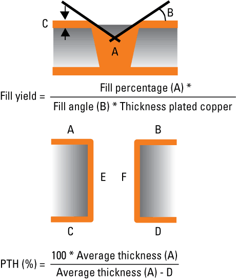
The Via Fill Yields (VFY) and through-hole metallization (PTH) metrics are calculated as shown in Figure 5.
The VFY takes into account not only the percentage of fill of the
microvia, but also the thickness of the plated copper on top of the
board and (in case of incomplete fill) the fill angle (B). The smaller
this fill angle, the easier it will be to fill the microvia with solder
or resin without air entrapment. Typically, yield values over 5%
represent good fill. For the through holes, the objective is usually
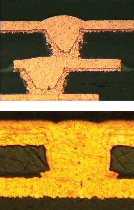
PTH > 80%. Some representative via-fills are seen in Figure 6.
|
|
|
|
As illustrated, the solderable surfaces of the pads no longer have
deep wells to trap air. Limiting the contribution of the microvia to
solder joint void formation has been the topic of many studies, and
there are several methods available to minimize the microvia’s
contribution.
Published Studies on Microvia Voiding
Several earlier studies on microvias and voiding have been published previously in 20035,6,7
and showed, among other findings, that copper-filled microvias
exhibited the best results in reducing voiding. Vias that were
completely filled showed less voiding than vias that were partially
filled, presumably because less entrapped air creates fewer voids.
Smaller via sizes were seen to create smaller voids than larger vias.
On the assembly side, soak profiles produced fewer voids than ramp
profiles. These studies were performed prior to the introduction of
low-voiding solder paste formulations.
The findings
of these studies provided an excellent basis for an investigation that
began in 2004 and finished up in late 2006. This study, which used the
simple two-step copper via fill technique previously described,
examined the effects of:
- Via presence and size
- Alloy system (tin-lead or lead-free)
- PCB finish
- Via filling
The complete report of the study8 can be obtained from the Surface
Mount Technology Association Web site (smta.org). Some key findings
from the study are discussed below.
Via Presence and Size
The test vehicle in the DOE was designed to compare pads with no vias,
4-mil vias, and 6-mil vias side-by-side on the same assembly. As
anticipated, the fewest voids were produced on pads with no vias at
all. More were produced on pads with 4-mil unfilled vias, and the most
were produced on pads with unfilled 6-mil vias.
Alloy System
Both
tin-lead and SAC305 alloy systems were used in the study. No mixed
metals were investigated. Devices with eutectic tin-lead balls were
soldered with tin-lead solder paste; likewise, devices with SAC305
balls were reflowed with SAC305 solder paste.
For
all four device types used in the study, the lead-free system performed
equivalently or slightly better with respect to void production. The
performance difference between lead-free and tin-lead was not
substantial, but the trend was consistent. This is an important fact to
note, because for many years, lead-free solder pastes were believed to
produce more voids than tin-lead. This was the case early in the
lead-free transition, when paste formulators were still climbing a
steep region of the learning curve. Most formulators now have at least
five years of lead-free experience under their belts, and modern
generation lead-free pastes can often rival the best-in-class
characteristics of their tin-lead predecessors in nearly every
performance category.
PCB Finish
Three
surface finishes were included in the study: OSP, ENIG and immersion
silver (ImAg). OSP and ImAg generally produced similar amounts of voids
that were less frequent and smaller than those produced with ENIG
finish.
Effect of Via Filling
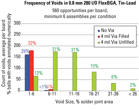
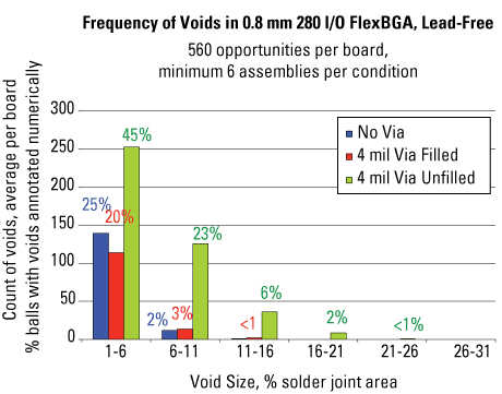
The most remarkable result was the effect of filling the vias with
copper. The investigators found it impossible to differentiate the
voiding performance between filled vias and pads with no vias at all,
regardless of device type or alloy system. The charts in Figures 7 and 8 show the voiding behavior of 0.8-mm FlexBGA devices.
|
|
|
|
As shown here, it is easy to visually differentiate the performance
of the unfilled vias from the other two test conditions. But it is not
so easy to discern a performance difference between the pads without
vias and the ones that had the vias filled. The data from these two
conditions were analyzed statistically, and it was determined that with
95% statistical significance, the voiding rates produced on pads with
filled microvias are equal to the voiding rates produced on pads with
no vias at all.
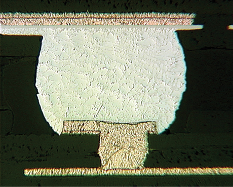
A cross section of a filled microvia is shown in Figure 9.
The via is filled with copper, and the surface of the pad is nearly
planar. There is no room for air to get trapped during the printing
process, thus no contribution from the microvia to solder void
production, and no concerns regarding void location based on final
finish.
|
|
Conclusions
HDI and microvia-in-pad technologies
have enabled the continuous migration to smaller, lighter, more
powerful electronics by enabling finer pitch I/Os, thinner circuit
boards and higher routing densities. For many years, their application
was relatively limited to portable devices, as high reliability and
high performance applications have not been nearly as eager to adopt
this technology as the portable providers. Today, HDI and
microvia-in-pad technologies are becoming more mainstream and (welcome
or not) are quickly becoming a fact of life for many designers and
assemblers, regardless of the end product they produce.
As with any forward step in technology, hurdles must be cleared on the
path to maturation. For many fabricators, those hurdles included
plating impediments, additional process steps and added cost. For
assemblers, those hurdles included solder joint starvation, solder
joint voiding and overall reliability concerns for the end product.
Many
of these concerns have been addressed, and numerous methods of
resolution are available. The specific solution of filling the vias
with copper plating in the same process as PTH plating tackles concerns
on three fronts: it provides better thermal and electrical design
characteristics when compared to existing technologies; it reduces
process steps in fabrication; and it eliminates excessive voiding in
board-level assembly. And it does it all within relatively short
plating times while offering simplified and consistent methods of
process control. Given that the major obstacles have been cleared, a
broad spectrum of electronics sectors can now employ HDI and
microvia-in-pad technologies and enjoy the cost and performance
benefits that they bring to the end product. PCD&F
Chrys Shea is R&D Applications Engineering Manager, Cookson Electronics Assembly Materials. She can be reached at This email address is being protected from spambots. You need JavaScript enabled to view it.. David Ormerod is Business Director, PWB Metallization, Enthone Inc. He can be reached at This email address is being protected from spambots. You need JavaScript enabled to view it..
Acknowledgements
The
most recent study cited above was a two year endeavor, and this article
is based on the findings of this activity. Many thanks to the
contributors of this study: Rahul Raut and Lou Picchione of Cookson
Electronics; Quyen Chu and Nicholas Tokotch of Jabil Circuit; and Dr.
Paul Wang of Microsoft.
References
1. Japanese patent application JP20002 19994(A); European patent application EP1152071A1.
2. IPC-6012B, Qualification and Performance Specification for Rigid Printed Boards, IPC, Bannockburn, IL, 2007.
3. Verbunt, D. Isik, U. Schmergel, Dr. J. Rasmussen: “Optimized
Vertical Process for Microvia Filling and Through Hole Metallization
under Production-like Conditions”, IPC, Anaheim, February 2005.
4. “Simultaneous Microvia Filling and Through-Hole Metallization,” A.Lachowicz et al, CPCA Proceedings, March 2006.
5. Grano, F, et al, “Impact of Micro-Via in Pad Design on Void Formation,” Proceedings of SMTA International, September 2003.
6. Harjinder, L. and Sundar, S, “Assembly Issues with Microvia
Technologies,” Proceedings of SMTA International, September 2003.
7. Singer, et al, “The Effect of Via-In-Pad Via Fill on Solder Joint Void Formation,” Proceedings of IPC Works, October 2003
8. Shea, et al, “BGA Solder Void Correlation to Via-In-Pad, Via Fill,
Surface Finish, and Lead-Free Solder – Final Report,” Proceedings of
the Pan Pacific Microelectronics Symposium, January 2007.
