Carbon Nanotube Patent May Portend More Moldable Electronics
CUPERTINO, CA – For years, R&D specialists have been working on carbon nanotubes as a means for electronic interconnection.
Last month, their work edged closer to the mainstream as a trio of Apple engineers was awarded a US patent for a bendable or flexible smartphone that uses carbon nanotube printed circuits.
A carbon nanotube is a tube-shaped material with a diameter about 10,000 times smaller than a human hair. They are outstanding heat and electricity conductors. They are also impressively strong, having been shown to be at least 100 times stronger than steel, at a small fraction of the weight.

The new patent, no. 9,485,862 describes an electronic device with carbon nanotubes patterned to form signal paths both on the substrates and interposed between polymer layers. The signal paths may resist cracking when bent. The description says openings in the polymer layer may expose metal solder pads on the carbon nanotube signal paths. Stiffeners may be used under the pads. Polymer materials in the flexible structure may be molded to form bends. Bends may be formed along edges of a touch sensor or display or may be formed in a flexible printed circuit.
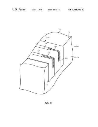
The carbon nanotubes are used to help prevent cracks in the signal lines traversing bent portions of a flexible substrate from disrupting signal flow; for example, see substrate 182 in the diagram. The inventors say the signals paths on the polymer layer (186 in the diagram) may be formed entirely from carbon nanotubes, or may include metal (166). Gap in the portion of layer 186 that traverses the bend at edge 174
help avoid metal signal line cracking To electrically connect metal signal lines on either side of the bend, a carbon nanotube segment (168) may bridge the gap in metal signal lines 166.
Configurations of the type shown in the figure may also be used to permit signal lines to traverse a hinge or other flexible joint.
Carbon nanotubes are flexible and are therefore resistant to cracking and undesired open circuit conditions due to bends. By providing flexible substrate 182 with carbon nanotube paths that cover metal paths in at least the portion of the metal paths that bend, the likelihood of undesired open circuit conditions in the signal paths is reduced, the inventors say.
The inventors are Ibuki Kamei, Timothy J. Rasmussen and Trent K. Do. They filed the application in August 2014.


