Power Integrity Analysis Using Free Software
Freeware has its limitations, but for some operations it is surprisingly effective.
Larger companies typically have a signal and power integrity department that performs power integrity analysis on development projects, and which has exclusive access to signal integrity software licenses. In these cases, these tools are not available to hardware design engineers. Often, the SI team engineering resources are only available with larger delays or on only one or two occasions during a project. Small companies generally lack SI teams; instead, hardware design engineers perform SI/PI analysis. Many small companies cannot afford to purchase SI/PI simulation software. So, were a hardware design engineer to need some quick simulation or need to experiment, they often simply have to give up getting any accurate SI/PI insight into their designs.
Here, it is explained how to perform PI simulations using freeware software. In his research, the author did not find a comprehensive and usable freeware SI tool, so the focus is on PI analysis. The software presented here are not specifically SI or PI programs, but generic circuit simulators or field-solvers.
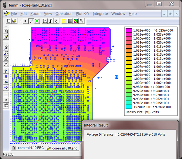
Figure 1. Voltage distribution.
DC voltage drop analysis using FEMM. For this, there is a freeware 2D finite element field-solver program called FEMM (Finite Element Magnetics Method) (femm.info). For a PCB power plane DC resistance, voltage drop or current distribution analysis, all that is needed is a 2D field-solver. A DXF version of the power plane, including all vias, can be imported, and then voltage drop can be simulated (Figure 1), DCR from voltage drop calculated, or current distribution visualized (Figure 2) to find weaker sports of the plane design. The simulation setup takes a lot of work, but hey, the software is free.
To analyze a PCB power plane in FEMM, create a new file as a “Current Flow Problem.” Next, set up materials (copper and air), conductors (VCC fixed voltage for the VRM – and ICC total current for the load). The DXF drawing might have to be edited before importing it to reduce the model complexity, which could be down with a free mechanical design tool like A9CAD. Even after importing it, further reduce the model, then convert all curves into 45⁰ lines to eliminate infinitely small features.
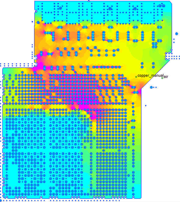
Figure 2. Current density distribution.
Typical values for setup: mm unit, 1Hz frequency, 5⁰ minimum angle, Sigma=59600000 for copper material but 0 for air, curve max segment 45⁰. Assign two materials (block labels), then select “default” for the air area to avoid having to define every one of the hundreds of vias and antipads to be air as well. Assign the conductors to all power vias of the load and the VRM source. Check the layout viewer in parallel to identify each via, as FEMM does not import net names. After simulation, measure voltage drop by drawing a line between the VRM and the load, then select “Integrate > Voltage Drop.” The DCR can be calculated by DCR = Vdrop / ICC. Using multiple layers to deliver the power allows us to simulate all layers separately, calculate DCR separately, then calculate the effective total DCR as parallel circuit effective resistance, as follows:
1/R_eff = 1/R1 + 1/R2 +...
Then, the total voltage drop in the system will be
V_drop = R_eff * I_Load.
It is useful to see which parts of the plane carry more current than others, so plane shape can be optimized to reduce DCR by eliminating hotspots. For this, select “View > Density Plot > |J|” in the menu. If the colors are not telling the story very well, change the red and blue thresholds.
If the PCB were designed in Cadence Allegro, many problems could be avoided in FEMM by considering these settings for DXF export: Enable etch layer and pins only, no vias. Enable “Display Plated Holes” and make “NC Drill Legend” and “NC Drill Figure” layers visible. In the NC Drill customization dialog set, match the symbol figure to the drills with the via drill size to “circle,” so we can see the vias as these circles.
Frequency domain power plane analysis using Sonnet Lite. For decoupling analysis we also need to know how well the power and ground plane pairs perform in the frequency domain. With free programs we cannot import a PCB layout design in for simulation, but we can draw a similar size and shape polygon. This should be good enough, as the main plane parameters that determine the AC performance are the dielectric thickness and the larger dimensions (resonant modes). The Sonnet software Lite version is freeware (sonnetsoftware.com) and has limitations, but is suitable for this purpose. Sonnet Lite Plus has DXF import, but it is not free, although it is cheap, costing a few hundred dollars (Figure 3). Sonnet Lite has a 1MB or 32MB (if registered) memory limit, and up to four ports can be assigned. For a 100x100 cell plane model, the 32MB option is ideal. We should use the Sonnet Lite to extract two port S-parameter models of the plane pair for further analysis. One port is needed for the VRM and one for the main load (BGA chip).
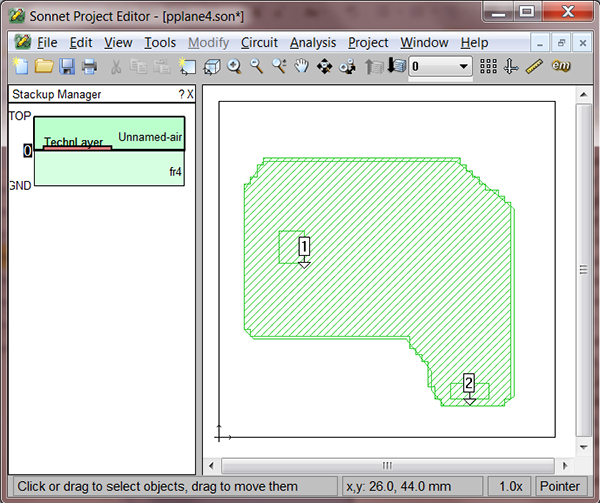
Figure 3. Sonnet Lite power plane model.
From the Circuit menu, set up the stackup, materials (dielectric layers and metal types) and other simulation parameters. Also, define a “circuit box” as needed for simulation (at Circuit > Box menu), which should be sufficiently large, for example 50 times thicker than the PCB, have cell size around 1mm, and 100x100 cells total size. Use the bottom plane of the box as ideal ground plane, and define one metal layer (called “0”) for the power plane. Select FR-4 material in between the power plane and the box bottom side, and air between the power plane and the box top side. For multiple power/GND plane pairs, generate separate S-parameter models for each. Draw the power plane shape on the layer called “0” (by Tools > Add Metallization > Draw Polygon from the menu. Make sure the plane edge does not touch the box edge, and the larger dimensions are accurate; measure them in the PCB layout design file. Draw two small polygons inside the plane: one for the voltage regulator and one for the load. Place simulation ports on the edges of the small polygons, then set their type to “Auto-ground.” The entire edge segment will become the port. Create a “Technology Layer” object for the plane geometry in Circuit > Technology Layers > Auto Create, then select copper as material and thickness, then name it. Set up the simulation parameters and the output file type from the Analysis menu. When the simulation is run, it will write the result into an “.S2P” Touchstone file. Other useful features are “Estimate Box Resonances” and “View Currents,” if enabled for simulation. The latter displays current distribution on selectable frequencies for resonance-hunting to help deciding capacitor placement and plane shape modifications.
Time domain power plane analysis using Faustus MEFiSTo-2D Classic. We can analyze plane waves and how they create resonances on the power planes using the MEFiSTo-2D Classic application (faustcorp.com). If we suspected that the plane resonates at a certain frequency, it can be simulated to see how the standing waves get created and at what locations, while trying to figure out how to eliminate them by changing the plane shape (Figure 4). Create a plane by drawing “Magnetic Wall” lines for the plane edges and rectangles around the whole structure with “Computation region” and “Animation Region.” Then place a “Source Region” for the main digital chip as a noise source. Set the source/excitation type (sin(f)), frequency and number of simulation steps (Total=50/[f*TimeStepDeltaT]), then run the simulation using the “++” icon to animate the plane wave propagation.
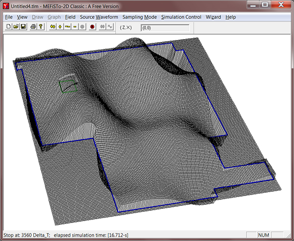
Figure 4. MEFiSTo-2D Time domain plane simulation.
Frequency domain complete system PI analysis using QUCS. The voltage regulator model in the template is a behavioral model that is a sub-circuit instantiated from a separate schematics page during simulation. The model does not look like an actual switching regulator, but it produces the same AC output impedance profile as the real regulator. The original circuit could not be included in a Spice-AC simulation. Parameters on the VRM (DC/DC) page have to be adjusted based on a few simple rules to achieve this before simulating the entire PDN system. To verify the parameter setup, compare the open control loop gain with the expected one from the controller chip’s datasheet or simulator tool. Simulate the VRM AC model on its own for output impedance or control loop gain in the QUCS template. (Figure 5)
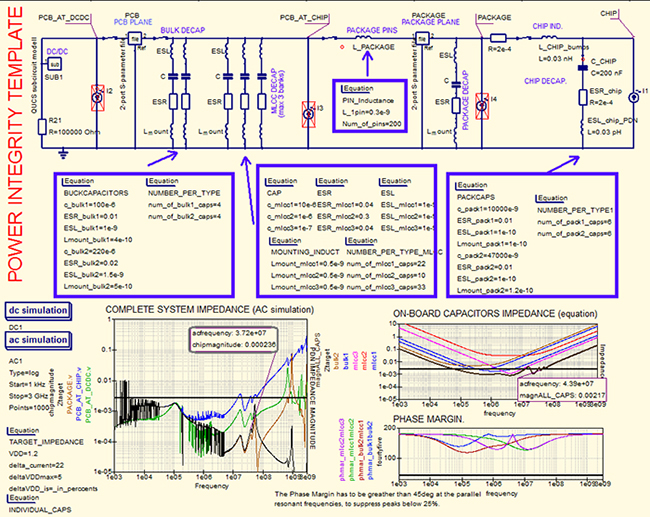
Figure 5. QUCS PDN model.
Another similar application is the Altera Power Distribution Network Design Tool or PDN Tool, which is an Excel calculator. The Altera tool can analyze a complete PDN impedance profile with parametric data entry. It models the PCB power planes as rectangles and probably applies analytical equations on it.
Freeware SI analysis programs. The free programs discovered for SI analysis only help a little. They cannot perform a full chip-to-chip IBIS-model-based or IBIS-AMI-based convolutional or channel simulation on S-parameter channels. Extracting an accurate-enough signal trace model, including return path, would require a non-limited 3D (or at least 2D) field-solver. Then a convolutional or channel simulation would be needed to connect the chip I/O buffer (IBIS) models with the channel S-parameter model. So far, all this can only be done using commercial software. The channel simulation is available for free from some chip vendors under NDA, but can only be used with proprietary chips.
Sonnet Lite can determine insertion loss or crosstalk for a simple geometry trace segment. Eispice can run an IBIS-model, ideal transmission line and passive termination-based simulations in text/command line mode. TNT-MMTL can calculate trace impedance with its built-in accurate 2D field-solver. The LC from Cray (under Linux) can extract S-parameters from PCB traces, although it is hard to use it in “quick” simulations. FastFieldsolvers extract parasitic inductance and capacitance of simple 3D structures like connectors, although the user has to draw the geometry. The LeCroy free S-parameter Viewer can view and assess S-parameter insertion loss and other profiles from simulations or measurements.
FEMM can also be used for very accurate impedance calculations on complex cross-sections, or to simulate per-unit-length crosstalk, or to visualize and measure the spread of the return current under a trace inside the reference planes (Figure 6). For impedance simulation on a given frequency, we have to simulate the same cross-section geometry/drawing in magnetic (to get R’, L’, and to visualize the return current) and current flow (to get G’, C’) modes, and then calculate the impedance with the calculator at buenos.extra.hu/download/Z0-rlgc.xls.

Figure 6. Return current spread visualization in finite element magnetics method.
In summary, various free software provides some very useful information about electronics designs. They require more clever ways to set up the simulation and interpret the results. It is much better than nothing, but commercial software is more substantial. For example, using an Agilent ADS or Hyperlynx LineSim instead of the QUCS would give a more realistic Z(f) curve without the noise caused by computation errors. Agilent Momentum and Ansoft SiWave provide accurate power plane models with imported CAD data with many ports compared with Sonnet Suites. The Cadence Allegro SI/PI options can even evaluate the effects of different decoupling capacitor placements. Hyperlynx PI could analyze DC voltage drop on multiple power planes in one run and without the tedious setup effort of the FEMM tool.
is a senior hardware design engineer at Fortinet (fortinet.com) and has a master’s in electrical engineering; This email address is being protected from spambots. You need JavaScript enabled to view it..


