Power Integrity and Power Distribution Design Tips
How to treat every power distribution system as a custom design.
Are you losing sleep over power integrity on your boards?
If so, this is for you.
I recently had the pleasure of presenting a webinar concerning power integrity. It was a primer on power distribution systems and how to address the issue of getting enough charge to high-frequency devices. This prompted sharing of some of the ideas that can be implemented immediately.
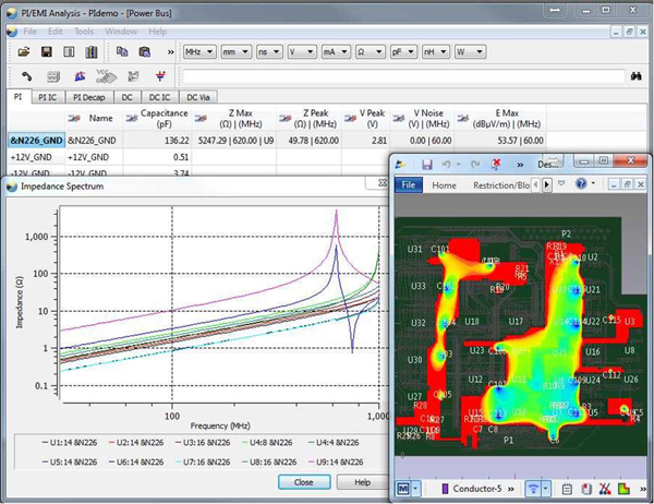
PCB power integrity is impacting design quality like never before. A power integrity problem can be difficult to detect and recreate, which can slow time to market.
A few steps can be undertaken today to improve the power integrity of a system. Here are my top tips:
- The power distribution system of each design must be treated as a custom design.
- Have power and ground planes ...
On adjacent layers.
With as thin a dielectric as possible.
As close to the surface as possible. - Between decoupling cap pads and the vias to the planes …
Surface traces as short and wide as possible.
Better: butt up via against the land or use via-in-pad. - Place capacitors (think minimizing current loop areas) ...
As close as possible to the package being decoupled.
On the same side (top) as the package.
Some caps under the BGA as well.

Figure 1. Power integrity problems are difficult to detect and recreate, causing delivery delays.
Griff Derryberry is a senior applications engineer at Zuken (zuken.com); This email address is being protected from spambots. You need JavaScript enabled to view it.. For more on this topic, see his webinar at http://pages.zuken.com/Webinar2-Registration.html.


