Creating a ‘Step Down’ PCB with PCIe Fingers on Both Sides
Meeting dimensional and signal integrity requirements while fitting standard slots.
Fabricators often create multilayer PCBs of various thicknesses, which may include PCBs with varying thickness in specific areas to accommodate a socket or edge connector. One example of this may be a “step down” PCB.
A step-down PCB is simply a multilayer PCB whose board thickness is reduced (stepped down) in a few places. The step-down is formed by employing stackups, in which some areas of the board are thinner than others. This is typically achieved by changing the number of layers in those regions.
PCIe fingers, also referred to as edge connectors or gold fingers, are gold-plated strips on the edges of printed circuit boards (PCBs), such as those on graphics cards or memory modules (Figure 1). A step-down PCB with PCIe fingers on both sides facilitates the physical connection between the PCB and its corresponding slot on a motherboard or other device, enabling the transfer of data and power. PCIe fingers enable for the PCB to connect to other components for signal and data transmission.
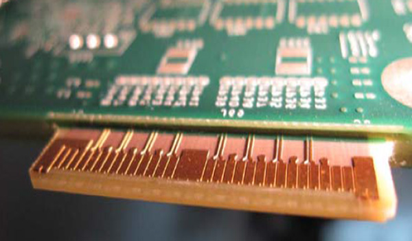
Figure 1. Step-down PCB with PCIe fingers, enabling connection to a motherboard.
PCBs with PCIe connectors must be 62 mils thick at the gold-plated fingers to fit properly into the slot. In impedance-controlled designs, a maximum of 16 to 18 layers can be used at this thickness. Even with special low-loss materials, however, the thinner line widths can affect product signal integrity (SI). To increase line widths, thicker dielectrics are needed, but this may not be possible due to board thickness limitations.
This becomes even more challenging when additional routing layers are required due to high routing density or the presence of extra components, which, in turn, increases the board thickness. As noted, if the board thickness exceeds 62 mils, it won’t fit into the connector. To solve this issue, manufacturers use a process called sequential lamination. Sequential lamination helps reduce PCB thickness in specific areas, ensuring that it meets design requirements while still fitting properly into the connector.
Which Side to Step Down?
Using this technique, PCB thickness can be reduced from one or both sides of the board in the connector area. Each option has its advantages; follow the fabricator’s recommendations to ensure good yield.
Step down from one side. Stepping the PCB thickness down from one side of the board typically leads to an unbalanced structure, which increases the risk of board warpage. Additionally, this type of construction usually requires more lamination cycles, making it more expensive. While we can handle the added cost, the main concern is the potential board warping, which could cause issues during the SMT assembly process. Having said this, stepping PCB thickness down from one side is an option, but it is not our choice. Figures 2 and 3 show a typical cross-section of a PCB that is to be stepped down from its top side, creating an unbalanced construction.
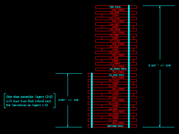
Figure 2. PCB cross-section to be stepped down from top side, creating an unbalanced construction.
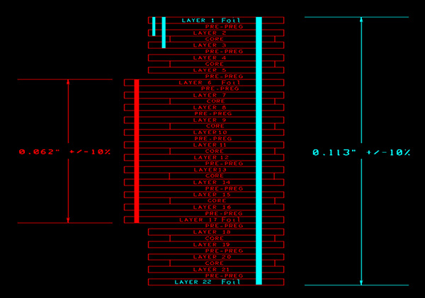
Figure 3. Cross-section of a balanced 22-layer PCB, stepped down from both sides of the board.
Step down from both sides. Figure 4 is a cross-section of a perfectly balanced 22-layer PCB, stepped down from both sides of the board. In this construction, top-side gold fingers shall be on L6, and bottom-side gold fingers shall be on L17.
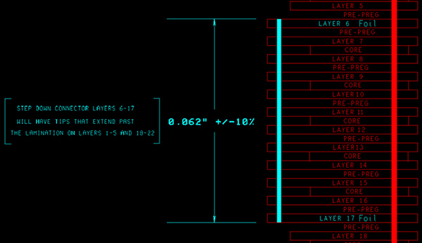
Figure 4. Closeup of balanced 22-layer board.
Manufacturing and Design Requirements
We have examined the example of a 22-layer PCB, where the layers are stepped down on both sides of the board. Specifically, the gold-plated fingers will be positioned in the middle part of the PCB, on layers L6 and L7.
To manufacture such PCBs, use sequential lamination, involving the following steps. (Because this part of the PCB will feature gold-plated tips, the board outline for all layers from L6 to L17 is shown in Figure 5. Thus, the board outline for the remaining layers, i.e., from L1 to L5 and L18 to L22, is shown in Figure 6.)
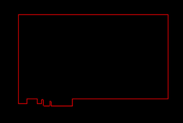
Figure 5. Board outline for layers 6 to 17 of the aforementioned 22-layer board.
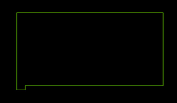
Figure 6. Board outline layers 1 to 5 and 18 to 22.
- 1. Following the standard manufacturing steps, all layers from L6 to L17 are etched, laminated, drilled and plated.
- 2. The remaining foils, etched cores and prepreg sheets (L1-L5 and L18-L22) are placed on both sides of the prelaminated L6-L17 section, and the entire stackup undergoes a final lamination cycle to form a single PCB spanning from L1 to L22.
- 3. Hard gold is electroplated onto fingers of L6 and L17.
- 4. The PCB is now ready for final drilling from L1 to L22, followed by plating and etching of the outer layers (Figure 7).
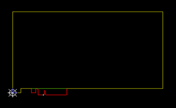
Figure 7. PCB is now ready for final drilling from L1 to L22, followed by plating and etching of the outer layers, resulting in the following appearance.
Finished PCB Dimensions
The finished PCB will exhibit the following dimensions:
- 1. Overall board thickness from top to bottom in the buildup area (L1-L22) is 0.113"±10%.
- 2. Layers 6-17 are stepped down at 0.062"+/-10% thickness.
- 3. Through-hole vias (L1-L22) require a minimum pad stack diameter of 0.020" and a drill size of 0.010".
- 4. The stepped-down connector area can have a pad stack diameter of 0.018" and a drill size of 0.008".
- 5. Drills and traces adjacent to the connector pads will be Ni/Au-plated, just as a plug-in connector.
- 6. The exterior surface finish can be any type.
- 7. Plated layers (L1, L6, L17, and L22) maintain a minimum 0.0035" spacing.
- 8. The remaining innerlayers maintain a minimum 0.003" spacing.
is chief executive of Rush PCB, a printed circuit design, fabrication and assembly company; This email address is being protected from spambots. You need JavaScript enabled to view it..


