The Via-in-Pad and Wrap Plating Process
How and why to achieve higher-density placement and routing.
PCB pin count and interconnect densities are increasing almost daily. Due to the associated high frequencies and speed, not only are impedance matching constraints challenging, but timing is also becoming more important. To add fuel to the fire, the size of the PCBs is getting smaller. Techniques are needed to create space and routing channels on these smaller PCBs. On one end, designers are under considerable pressure to create a design that can meet all the target functionalities. Conversely, PCB manufacturers are facing similar challenges in developing fabrication and assembly processes that can guarantee a reliable product with minimum tolerances.
Via-in-pad is a printed circuit board technology that permits SMT components to be placed with greater density and helps achieve higher interconnect density. In a typical PCB routing technique, escape traces are drawn from the component leads, and then escape vias are used to transition to the next routing layers. These escape traces and their vias require extra space. With via-in-pad technology, the via is inserted on the pad of the component, helping save space and achieve higher-density placement and routing.
This detailed document is intended to demonstrate via-in-pad from a manufacturing perspective.
Via-in-pad (Figure 1) is
- A surface mount pad that serves double duty as a surface mount pad and a via hole
- A surface mount pad with a via underneath, and
- Can be a double-sided via, a multilayer via or a blind via.
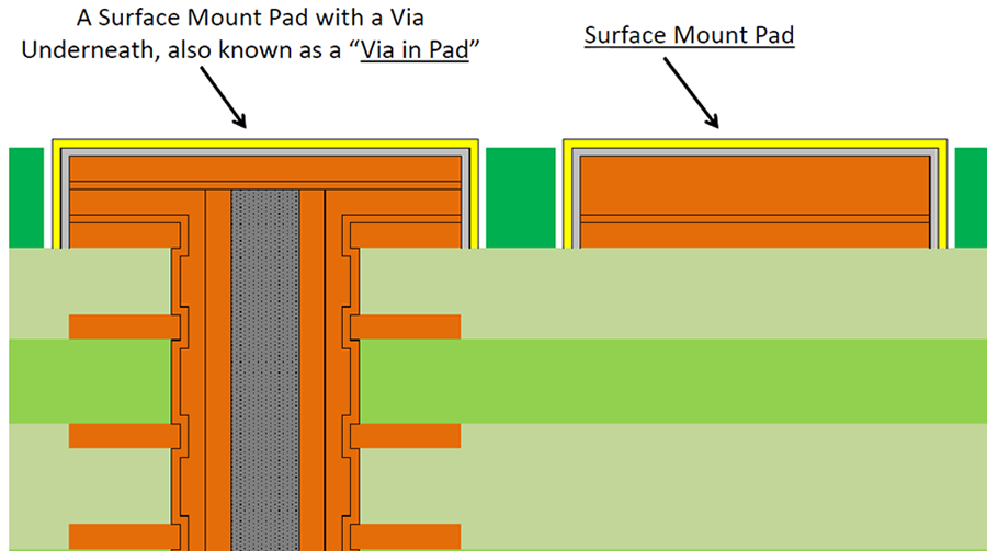
Figure 1. Cross-section diagram of a via-in-pad.
In terms of use, via-in-pad
- Increases component density
- Serves as a via and as a surface mount pad for a component.
Construction. Our standard process for constructing single wrap via-in-pad is shown. We will also pay attention to certain aspects of processing. For clarification, we are going to consider an eight-layer through-hole PCB construction (Figure 2).
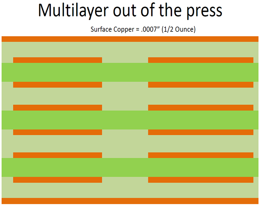
Figure 2. An eight-layer PCB out of the press.
When via-in-pad is manufactured, all other plated and non-plated holes are separated (Figure 3). Only holes for via-in-pad are drilled. This isolates the via-in-pad holes and simplifies the via fill process later. After via fill is complete, the remaining holes are drilled and final image processes.
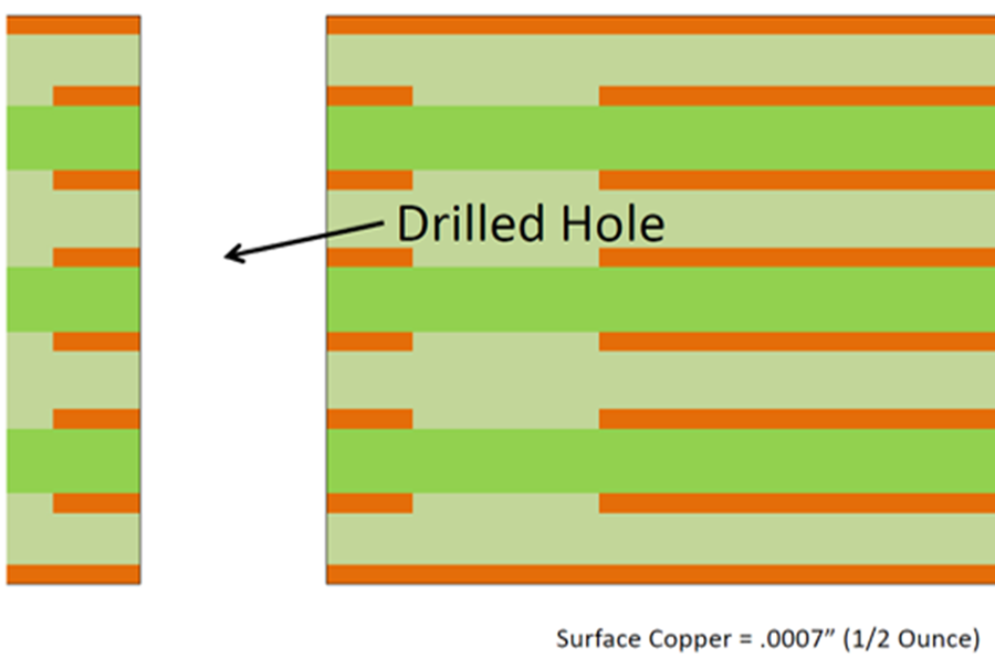
Figure 3. Drilling diagram.
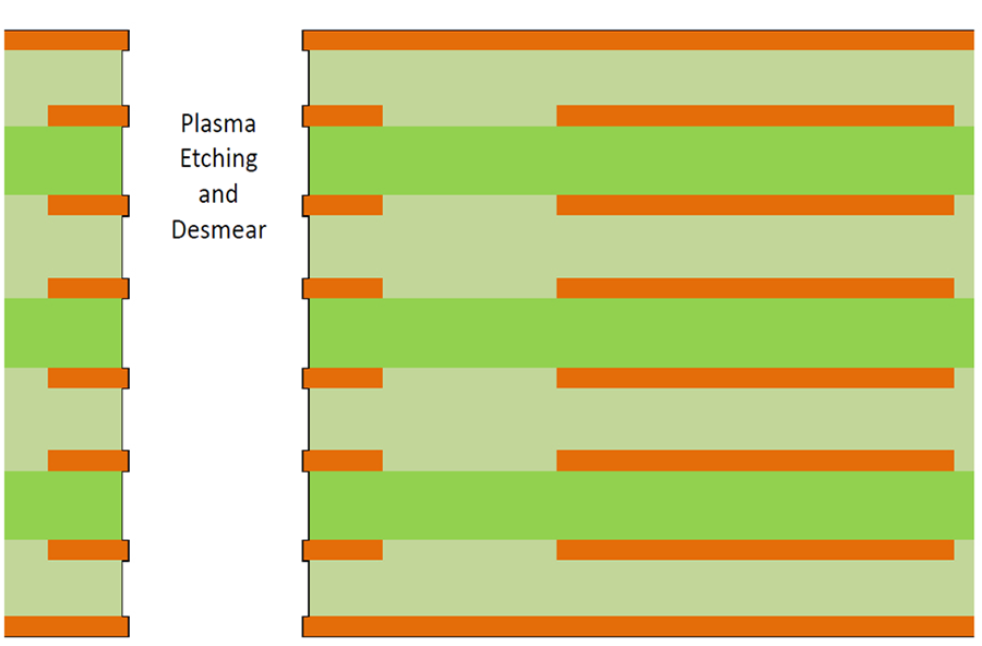
Figure 4. Drilled holes are cleaned by plasma etching to avoid resin smear.
Electroless plating. To form a conductive path in a hole barrel, an electroless copper plating process is carried out (Figure 5). This forms a very thin layer of copper inside the hole barrel, merely 0.0003 mils, which later will help achieve the process of electroplating.
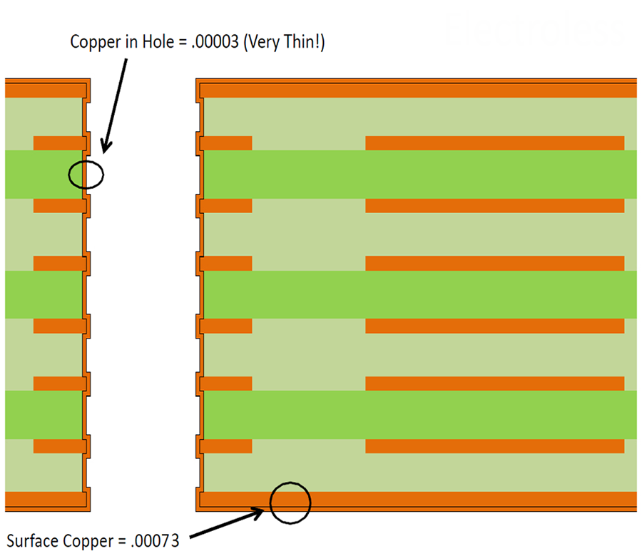
Figure 5. Electroless copper plates the hole barrel.
Electroplating (wrap plating). Electroplating adds more copper to hole walls; it adds approximately 0.53 mil, resulting in added thickness of copper to the cylinder of the hole barrel (Figure 6). Per IPC Class 3, the target copper thickness in the hole is 0.0013" (1.3 mil).
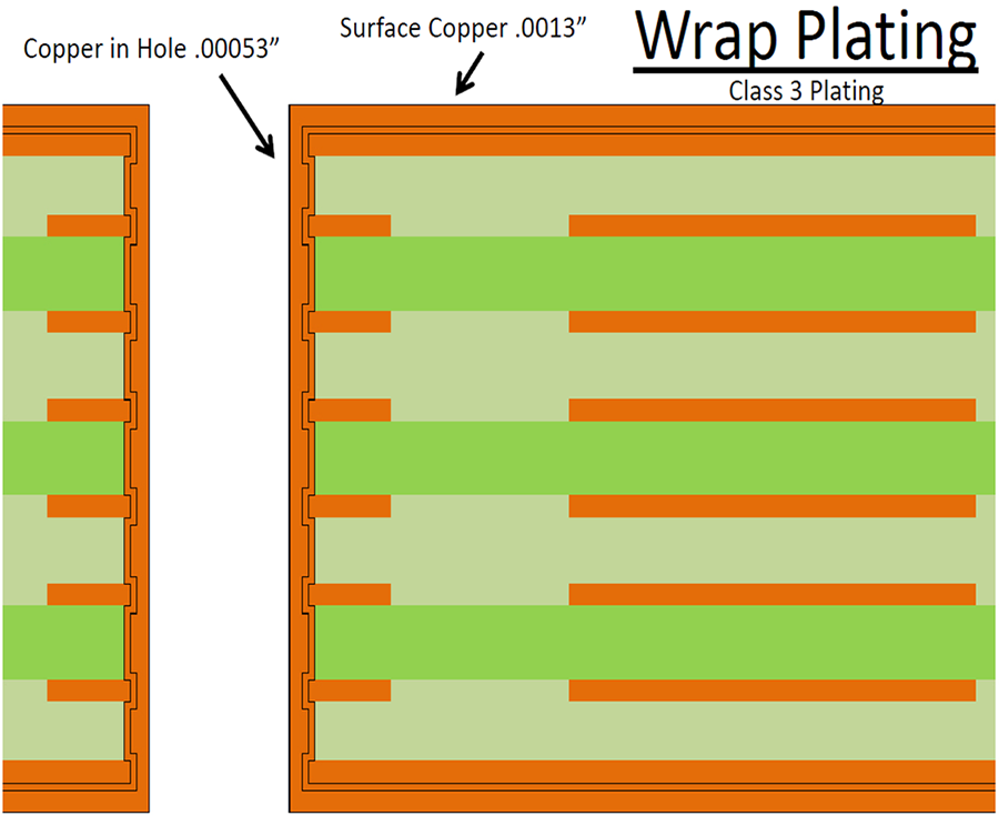
Figure 6. Example of wrap plating.
Wrap Plating
Wrap plating describes electrolytic hole plating deposition that continuously extends onto the surface from a plated via structure; essentially, copper plating from the hole that wraps around the surface foil. It is performed without any image defined by the photoresist.
Panels are taken from the deposition line and wrap-plated. It is the same process as flash plating, except more copper is added by extending the plating time. Flash plating adds about .00015", while wrap plating adds 0.0003"-0.0006" (2X to 4X more copper). Fabricators wrap plate the minimum amount to keep the thickness of the copper on the surface to a minimum so that etching is easier.
Wrap plating was introduced in IPC-6012B Amendment 1. Its sole purpose is to increase via-in-pad reliability in the field. Without wrap plating, the surface plating can be separated from hole plating (Figure 7).
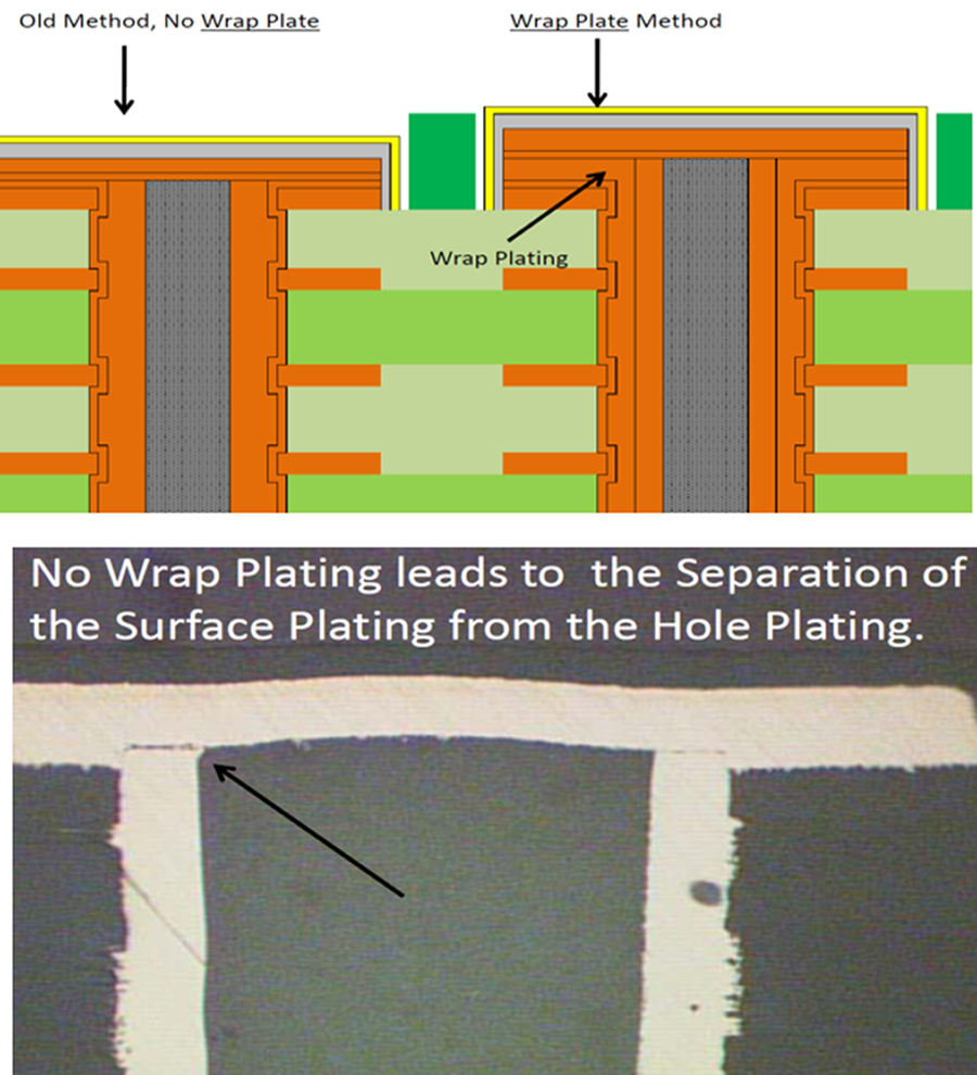
Figure 7. Via-in-pad without wrap plating (left) and with it (right).
Button (Spot) Plating
Button (spot) plating is the process of plating copper only in the holes and on pads (Figure 8). Applying plating resist and image, copper is again electroplated to achieve the desired thickness of copper in the hole. Plating resist covers the entire PCB area, exposing via-in-pad locations only along with their copper pads on outer layers.
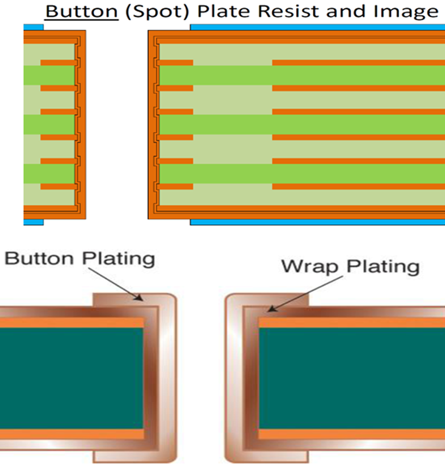
Figure 8. Button plating versus wrap plating.
Button plating is carried out to achieve the desired copper thickness in the hole barrel (Figure 9). When wrap plate is performed, only the minimum amount of copper required for the wrap plate is put in the hole and on the surface (plus a little extra to compensate for planarizing). Button plate, on the other hand, brings the thickness of copper in the hole up to the finished requirement without adding extra copper to the surface.
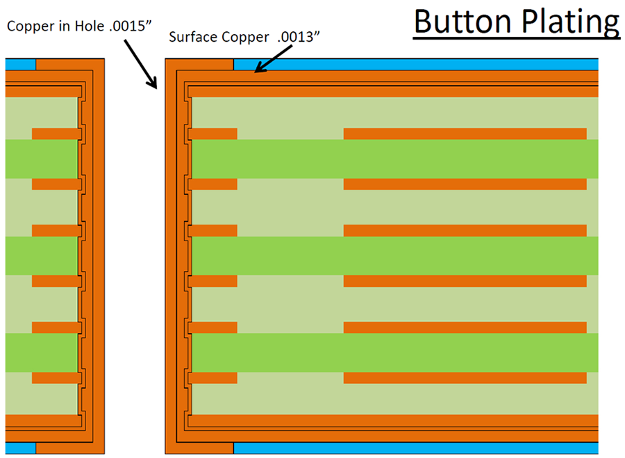
Figure 9. Button plating is performed to increase the copper in the hold but not on the surface.
To distinguish, wrap plate goes in the hole and on the surface, but button plate goes only in the hole and on the pad, not the entire surface. So, to build up the correct amount of copper in the hole before via fill, we first wrap plate, then button plate.
Figures 10, 11 and 12 show the subsequent basic fabrication processes.
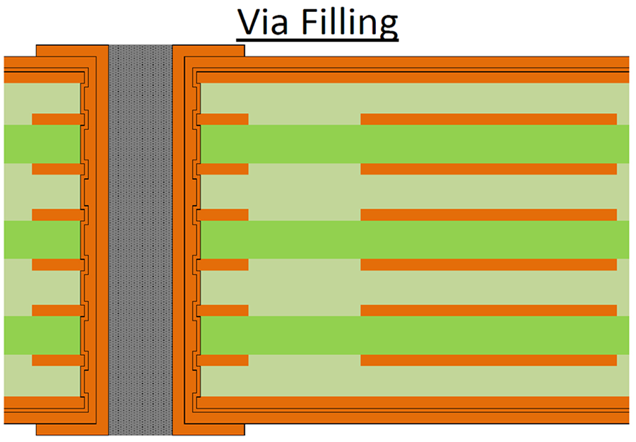
Figure 10. Following plating, vias are filled …
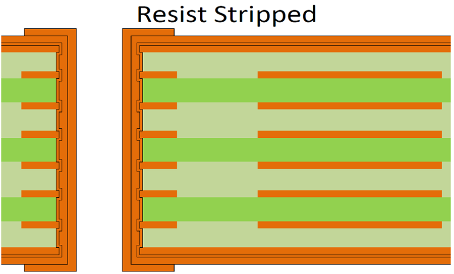
Figure 11. … Then resist is stripped from the board …
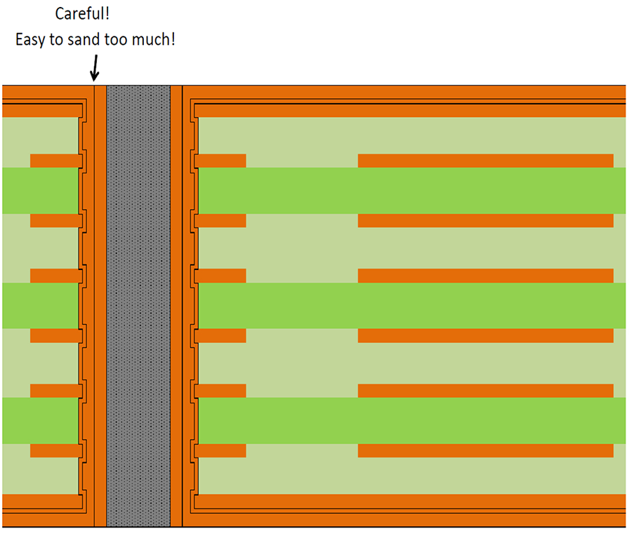
Figure 12. … Followed by a planarization step to remove excess copper.
Planarization
Planarization removes the surface copper from the button plating process, leaving a perfectly flat surface. Since fabricators plate as little copper on the surface as possible to aid in etching.
Generally, fabricators try to add only 0.0001" to 0.0002" extra copper to permit for losses at planarization. Because fabricators plate only an extra 0.0001" during wrap plating to permit planarizing, copper must be measured frequently to maintain minimum wrap requirements.
Remaining Fabrication Processes
Following planarization, the remaining holes are drilled (Figure 13), then the board undergoes a second plasma etching process (Figure 14), followed by a second electroless copper stage (Figure 15). Then the plating resist is added (Figure 16) and final imaging takes place, followed by final copper plating (Figure 17). Tin plating (Figure 18) then occurs, followed by resist stripping (Figure 19), etch image (Figure 20), and tin stripping (Figure 21). Then, solder mask is applied (Figure 22) and immersion gold plating takes place (Figure 23).
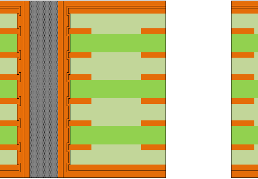
Figure 13. Drilling of remaining holes.
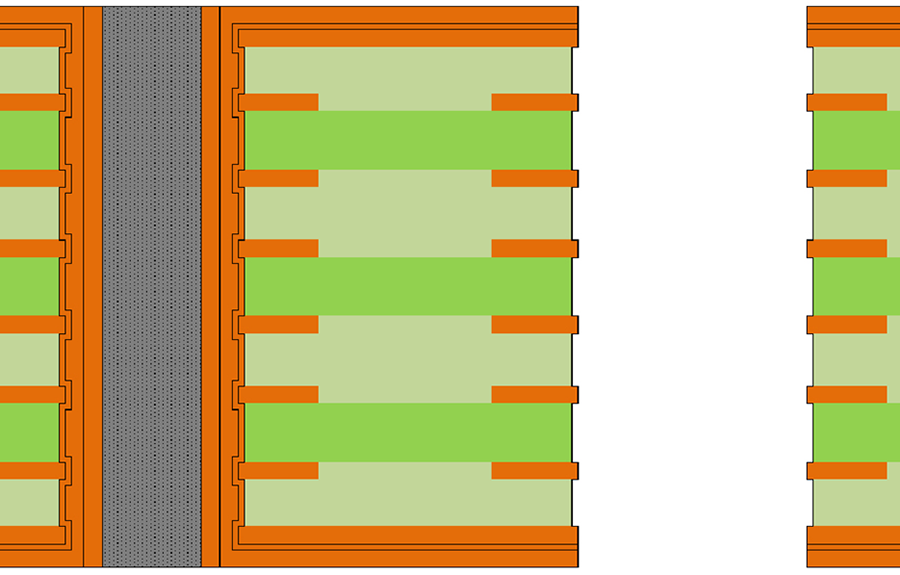
Figure 14. Second plasma etching.
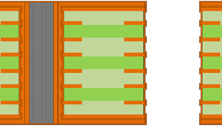
Figure 15. Second electroless copper stage.
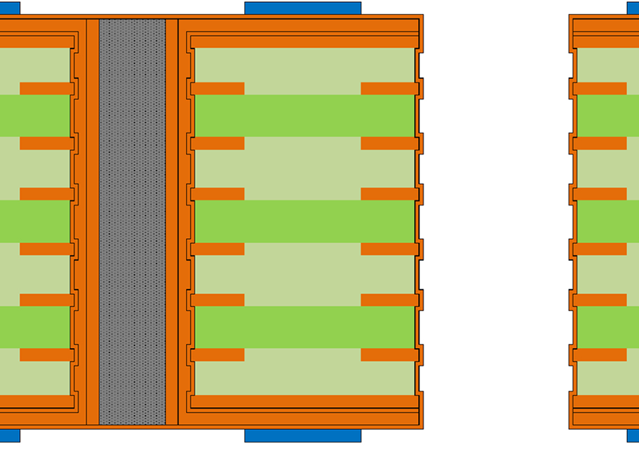
Figure 16. Plating resist is added.
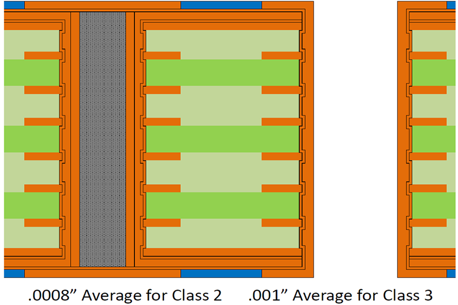
Figure 17. Final copper plating.
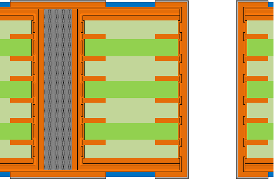
Figure 18. Tin plating.
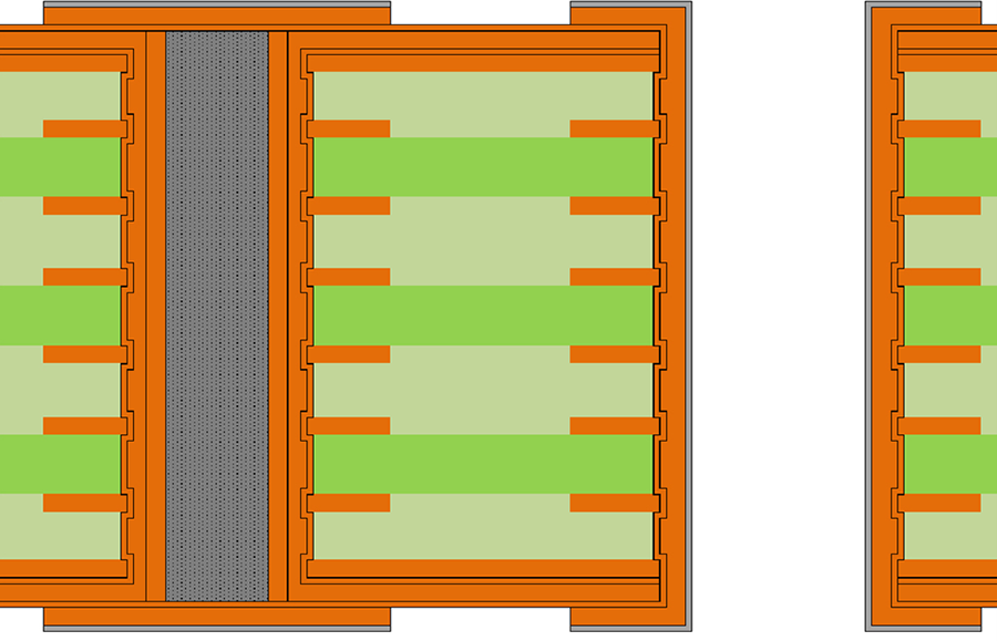
Figure 19. Resist stripping.
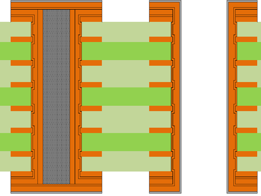
Figure 20. Etch image.
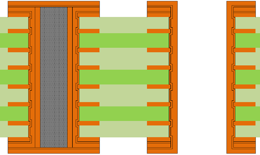
Figure 21. Tin stripping.
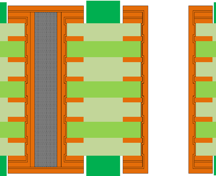
Figure 22. Solder mask application.
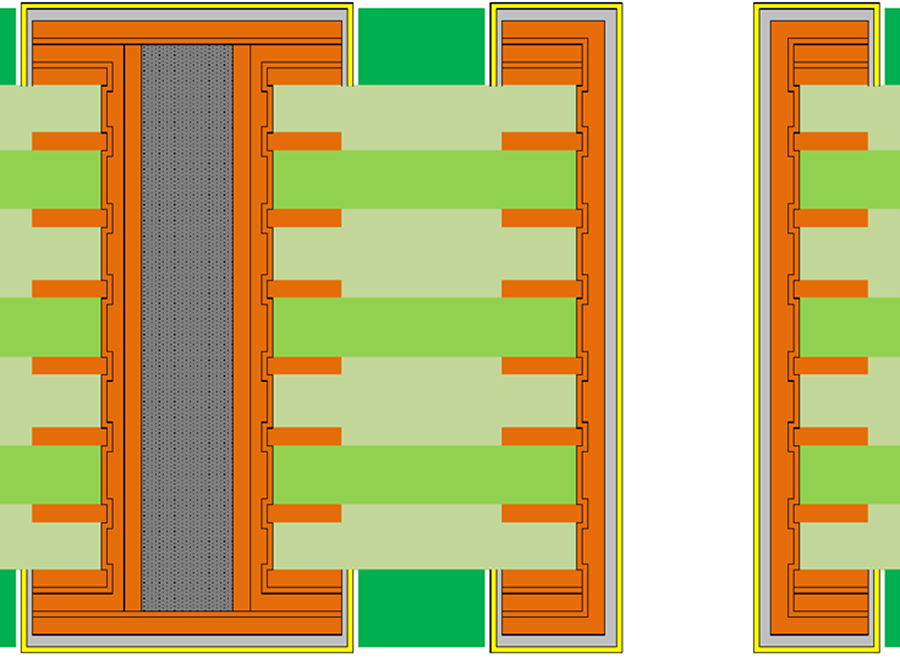
Figure 23. Immersion gold plating.
The standard procedure for via fill is shown in Figure 24.

Figure 24. Standard procedure for via fill.
is chief executive of Rush PCB Inc., a printed circuit design, fabrication and assembly company (rushpcb.com); This email address is being protected from spambots. You need JavaScript enabled to view it..


