Balancing Stackups and Circuitry
A symmetrical build is one of the keys to minimize board warpage.
A stackup’s construction should be balanced to keep board warpage within IPC specifications. In general, the following parameters must be symmetrical with respect to a fictitious center plane of the board:
- Dielectric thickness
- Buildup of the dielectric
- Pattern density (layer to layer)
- Thickness of copper foil
- Number of layers.
Figure 1 shows a symmetrical eight-layer build. The following notes clarify points on symmetry from the numbers shown on the stackup in the figure.
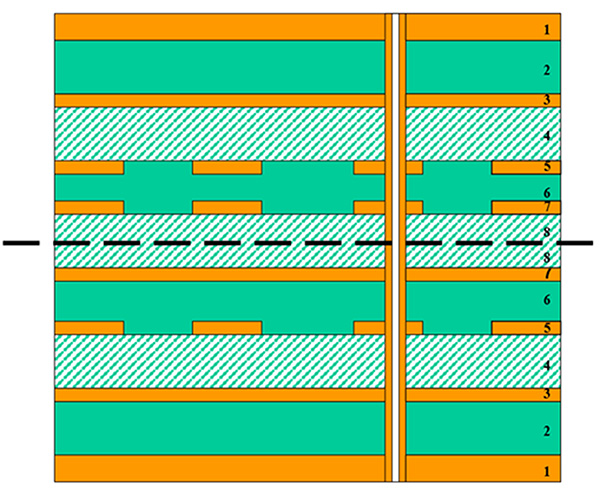
Figure 1. An illustration of symmetrical features in a stackup.
- This is the base copper weight of outer layers, where the starting foil thickness for each side must be identical and is typically 0.5 oz.
- Identical prepreg plies at these locations are highly recommended. Use of the same prepreg throughout the stackup will improve manufacture and reduce mistakes in this manual layup process.
- Copper plane layers should be the same copper weight, typically 1 oz.
- Identical cores are highly recommended to improve manufacturability.
- Copper signal layers should be the same weight, typically 0.5 oz.
- Identical prepregs are highly recommended, and could be different from those in note 2 to accommodate impedance constraints or overall PCB thickness.
- Innerlayer plane and signal layers can be different provided two criteria are followed. First, the copper weight must be the same. Second, the signal layer must have even copper distribution. Thieving pads may be added to help achieve copper balance with the symmetrical plane feature. Doing so helps to avoid excessive resin loss during lamination.
- The fictitious center of the board is in the middle of this core. This material could be different from the core in note 4 to accommodate impedance constraints or to meet the overall thickness requirement.
Core and Prepreg Recommendations
Within a given design, minimize the number of different cores and prepregs. And across all designs, standardize and minimize the number of different cores and prepregs used.
Copper Weight Recommendations
- 0.5 oz. outer layers
- 0.5 oz. or 1 oz. innerlayers
- Finer geometry may require thinner copper
- The most common cores have the same copper weight on both sides. This is recommended and these are most likely to be in stock for PCB fabrication.
Thicker innerlayers are sometimes required for heat dissipation or current carrying capability. Copper thicknesses of 2 oz. or more have limitations on minimum geometries.
Hybrid Construction
For cost reasons, use low-loss material only where required in the design, with cheaper material for general purpose routing and planes. Our experience with mixed substrates (PCBs with more than one material) has proven mixing materials is not as easy as it appears. Be aware of the risks and possible alternatives before proceeding. Because of issues with this type of build, it is recommended only on an exception basis. The following are points to consider before choosing a hybrid construction:
- Ensure a detailed cost understanding of a mixed material build, compared to one with high-performance cores all the way through. Generally, it only makes sense if three-quarters or more of the board thickness is the cheaper material.
- Research the supplier’s claims that they have experience with the requested hybrid construction. Inquire how many parts they have done. The board could be their R&D project. Be careful.
- The supplier must have UL approval for each specific mix of materials. If UL approval must be obtained, it can significantly delay the PCB turnaround time.
- Be aware of quality issues with this type of build beforehand, as it can be difficult to determine the actual root cause of the problem.
- Never rely on a single vendor. Always get input on hybrid builds from additional sources.
Hybrid Materials
Be aware of the following material properties and their implications for hybrid materials:
- Glass transition temperature
- Coefficient of thermal expansion, particularly z-axis expansion
- Dimensional stability
- Process incompatibility between materials.
is chief executive of Rush PCB Inc., a printed circuit design, fabrication and assembly company (rushpcb.com); This email address is being protected from spambots. You need JavaScript enabled to view it..


