State-of-the-Art Technology Flashes - Updates in silicon and electronics technology.
Updates in silicon and electronics technology.
Ed.: This is a special feature courtesy of Binghamton University.
Photovoltaic cell works at night. University of California researchers have developed a photovoltaic cell that can function at night. The cell can generate up to 50W/sq. m. at night, about 25% of what conventional solar cells generate in daytime. They currently are improving the output power and efficiency of the devices. The cell operates in reverse to a normal solar cell. An object that is hot compared to its surroundings will radiate heat as infrared light. The device can work during the day by blocking direct sunlight. Hence, this new solar cell could potentially operate around the clock. (IEEC file #11548, Science Daily, 1/29/20)
“Stretchy battery” for wearables. Researchers at Stanford University have developed a stretchy battery useful for wearable electronics. The battery can be stretched to twice its original length without any power loss. The polymers in lithium-ion batteries that conduct negative ions toward the battery’s positive pole are in the form of gels housed in a rigid casing. By providing a power source that could stretch and bend, wearable electronics can be more comfortable. (IEEC file #11547, Electronics Weekly, 1/29/20)
To continue reading, please log in or register using the link in the upper right corner of the page.
{!guest}
“Tattoos” with active electronics. Researchers from Duke University have developed a process to “print” flexible electronic patches with embedded TFTs directly onto the skin. This “print-in-place” technique for electronics can work on delicate surfaces, including paper and human skin. Unlike other printed electronics that require multiple layers supported by special treatment after each layer, this approach is much more direct. The breakthrough could lead to tailored biosensors for biomedical applications, including patient-specific biosensors. (IEEC file #11551, Electronic Design, 1/31/20)
Bionic chip to treat chronic diseases. Researchers from the University of Bath have developed the first artificial digital neuron (Bionic Chip) with the aim of restoring lost brain functions by repairing nerve circuits. They plan to use these chips to treat neurodegenerative diseases such as Alzheimer’s disease. The electrical properties of biological cells have long been studied to understand intracellular dynamics. The difficulty of measuring microscopic parameters that control the dynamics of ionic currents and the nonlinearity of ionic conductance has so far hindered efforts to construct quantitative computational models. The growing attention to implantable bioelectronics for the treatment of chronic diseases is driving technology toward low-power solid-state analog devices that accurately mimic bio-circuits. Analog asynchronous electronics is the most promising way to integrate raw nerve stimuli instantly, regardless of the size. (IEEC file #11571, EE Web, 2/6/20)
CMOS IC integrates quantum dots with conventional electronics. Leti researchers have developed a CMOS IC that integrates quantum dots on conventional electronic devices and elements. The chip was fabricated on a 28nm FD-SOI process, which integrates analog and digital functions. The target applications are instrumentation needs for a quantum accelerator. Beyond the need to obtain reliable, entangled and coherent quantum bits (qubits) on silicon, the goal is ultimately to produce electronics capable of routing numerous signals to address a matrix of several hundred qubits. The results can also be used for non-silicon quantum devices. (IEEC file #11589, Electronics Weekly, 2/19/20)
Low-cost manufacturing of flexible electronics using “remote epitaxy.” MIT researchers have developed a low-cost process called “remote epitaxy” to manufacture flexible electronics. The process involves growing thin films of semiconducting material on a large, thick wafer of the same material that is covered with an intermediate layer of graphene. After manufacturers grow the semiconducting film, they can peel it away from the graphene-covered wafer and then reuse the wafer. Hence, they can copy and peel away any number of thin, flexible semiconducting films, using the same underlying wafer. (IEEC file #11566, MIT News, 2/5/20)
3D-printing of perovskite nanostructures. University of Hong Kong researchers have developed a method to print perovskite nanostructures in three dimensions. The method uses a femtoliter meniscus of precursor ink formed on a nanopipette to localize and guide solution-mediated perovskite crystallization in mid-air, enabling nanoscale and freeform 3-D printing. Organic–inorganic metal halide perovskites have emerged as a promising optoelectronic material with exceptional structure and property tunability. This new generation of functional materials possesses excellent properties such as large optical absorption, long carrier diffusion length, high carrier mobility, and a low-cost solution production process. The ability of this method to tailor such nanostructure’s dimensions with an on-demand, minimalist manner could contribute to scientific research for fundamentals of perovskite-based material. (IEEC file #11575, Nanowerk, 2/11/20)
Stress-relief substrate helps OLED stretch. Researchers from KAIST (Korea Advanced Institute of Science and Technology) have created stretchable, compliant OLEDs that maintain their performance, even under high-strain deformation. The stress-relief substrates utilize pillar arrays to reduce the stress on the active areas of devices. The substrate also has relief island structures that relieve the stress at the bridges in the devices. A patterned upper substrate with bridges makes the rigid substrate stretchable, while the pillars decentralize the stress on the device. (IEEC file #11608, Science Daily, 2/28/20)
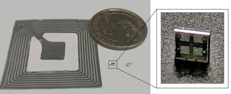
Battery-free ID chip combats counterfeiting. Researchers at MIT have invented a tiny cryptographic ID tag to verify authenticity in products, including integration into larger silicon chips. The millimeter-sized ID chip integrates a cryptographic processor, an antenna array, and photodiodes for power. Counterfeiting is a huge problem, estimated at $2 trillion worth of counterfeit goods. The new ID tag solves many of the challenges that come with today’s wireless ID tags. Examples include RFID tags too large to fit on small products, such as medical components, automotive parts, or silicon chips, with limited security measures. (IEEC file #11611, Electronics Products, 3/2/20)
Turning colored pigments into electronics. Queensland University researchers have developed a family of organic pigments set to drive the future of electronic devices. The organic pigments called diketopyrrolopyrrole (DPP) are carbon-based organic materials used for their color as dyes and for their charge transporting and optoelectronic properties. Another class of an orange dye called anthanthrone (ANT) could be used in the future for “perovskite” flexible solar cells built into curtains, sail shades or clothing. One of the advantages of pigments with electronics is they can be printed on a large array of materials, such as materials for solar cells, transistors, and sensors for medical devices inserted in the body to technology products designed to break down. (IEEC file #11610, Printed Electronics World, 3/4/20)
Market Trends
Phase-change and MRAM market forecasts. Market research projects 3-D XPoint (Intel-phase change material) and STT-MRAM (spin-transfer torque MRAM) will lead a $6 billion market for emerging memory technologies in 2025. The NVM (non-volatile memory) market will grow to over $4 billion in 2025. Two key segments will drive it: low-latency storage (enterprise drives) and persistent memory such as NVDIMMs (non-volatile dual inline memory module). The embedded emerging NVM market is projected to grow at a CAGR of 118% between 2019 and 2025 and reach more than $2 billion by 2025. (IEEC file #11605, Electronics Weekly, 2/27/20)
Printed sensor market forecast. The printed sensor market is projected at $8.63 billion at a CAGR of 6.62% during the period of 2020 to 2025. Printable sensors are a low-cost alternative to the silicon sensors due to the increasing demand application areas for flexible, stretchable, mass-manufacturable, and versatile printed sensors. Europe is the largest market for printed electronic sensors owing to increasing demand for medical industry printed technology. Adding to demand is the growing development toward human-machine interface, nano-dimension materials, and point-of-care devices. (IEEC file #11564, Research and Markets, 2/4/20)
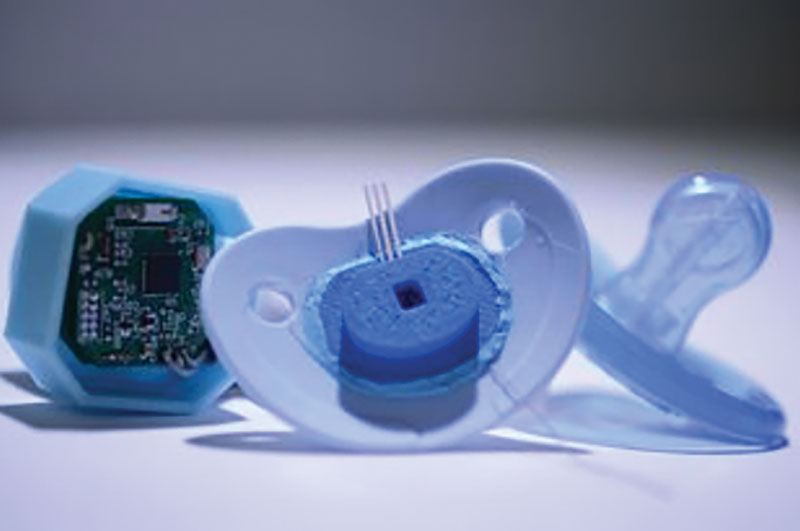
Pacifier to monitor infant health. University of Alcalá and University of California researchers have created a sensor for baby pacifiers. The prototype is made to test glucose levels. The sensor and electronics are kept on the outside of the pacifier, so there’s no risk to the baby or sensor. A small channel in the nipple collects saliva and gets pumped up to the glucose sensor. To prevent the saliva from reentering the baby’s mouth, plastic valves keep the flow unidirectional. Other metabolic diseases such as phenylketonuria and tyrosinemia can be monitored as well. (IEEC file #11611, Mechanical Engineering, 3/3/20)
Biometrics market to exceed $37.2 billion by 2024. The global biometrics market was $16.7 billion in 2018 and is projected to exceed $37.2 billion by 2024, a CAGR of 14% from 2019-2024. Biometrics refers to a technological authentication method utilized in information assurance for secure entry, data or access. It relies on scanning physical or biological characteristics, such as the face, DNA, fingerprint, iris, retina, etc., which are difficult to forge. It provides more accurate identification and lowers the risk of unwanted intrusion. As a result, biometrics technologies are widely used in schools, colleges, banks, public libraries, corporate and government offices, and consumer electronics including smartphones and tablets. (IEEC file #11618, Global SMT & Packaging, 2/26/20)
Recent Patents
Semiconductor device assembly with pillar array (assignee: Micron Technology), patent no. 15/830,839. A semiconductor device assembly and method of forming a semiconductor device assembly includes a first substrate, a second substrate disposed over the first substrate, at least one interconnect between the substrates, and at least one pillar extending from the bottom surface of the first substrate. The pillar is electrically connected to the interconnect and is located adjacent to a side of the first substrate. The pillar is formed by filling a via through the substrate with a conductive material. The first substrate may include an array of pillars extending from the bottom surface adjacent to a side of the substrate that is formed from a plurality of filled vias.
PCB that provides a direct thermal path between components and a thermal layer (assignee: Adura LED Solutions), Pub. no. US10531556. A method of assembling a component to a printed circuit board that includes a thermal layer and a circuit layer separated by a dielectric layer. The circuit layer includes circuit pads that correspond to terminal surfaces on the component. The dielectric layer includes an aperture that exposes a portion of the thermal layer that corresponds to a thermal pad on the component. Solder paste is applied to the circuit pads and the exposed thermal layer. Lower surfaces of the solder paste are in contact with the circuit pads, and the thermal layer and upper surfaces of the solder paste are substantially coplanar. The component is placed on the solder paste.
Heat-activated conductive spinel materials for PCB via overcurrent protection (assignee: IBM Corp.), patent no. 10,531,562. A process of utilizing a heat-activated conductive spinel material for PCB via overcurrent protection includes forming a PCB laminate structure that includes a spinel-doped insulator layer having a heat-activated conductive spinel material incorporated into a dielectric material as a spinel-based electrically non-conductive metal oxide. A sensing via is formed in the PCB laminate structure at a location that is proximate to a power via in the PCB laminate structure. The sensing via is electrically isolated from the power via by a region of the spinel-doped insulator layer and is electrically connected to a monitoring component configured to detect current flow through the sensing via.
Methods of forming a vertical semiconductor diode using an engineered substrate (assignee: QROMIS Inc.), patent no. 10,535,547. A semiconductor diode includes an engineered substrate, including a substantially single crystal layer, a buffer layer coupled to the substantially single crystal layer, and a semi-insulating layer coupled to the buffer layer. The semiconductor diode also includes a first N-type gallium nitride layer coupled to the semi-insulating layer and a second N-type gallium nitride layer coupled to the first N-type gallium nitride layer. The first N-type gallium nitride layer has a first doping concentration, and the second N-type gallium nitride layer has a second doping concentration less than the first doping concentration.
Binghamton University currently has research thrusts in healthcare / medical electronics; 2.5-D/3-D packaging; power electronics; cybersecure hardware/software systems; photonics; MEMS; and next -generation networks, computers and communications. The S3IP Center of Excellence is an umbrella organization comprising five constituent research centers.
Integrated Electronics Engineering Center (IEEC) is a New York Center of Advanced Technology (CAT) responsible for the advancement of electronics packaging. Its mission is to provide research into electronics packaging to enhance partners’ products, improve reliability and understand why parts fail. More information is available at binghamton.edu/ieec.
Register now for PCB West, the leading conference and exhibition for the printed circuit board industry! Coming this September to the Santa Clara Convention Center. pcbwest.com


