Monocoque Printed Circuits
Webster's defines Monocoque as follows:
1: a type of construction (as of a fuselage) in which the outer skin carries all or a major part of the stresses
2: a type of vehicle construction (as of an automobile) in which the body is integral with the chassis
Webster's does not consider a third definition: a new multi-functional circuit system. This week’s newsletter will consider the third definition.
During my trip to Taiwan, a local flex circuit manufacturer introduced me to a new printed circuit technology. The circuits are very different from typical rigid circuit boards because they have 3-D structures. The final product is not a flexible circuit because it has no flexibility. The manufacturer calls it a thermo-formed printed circuit.
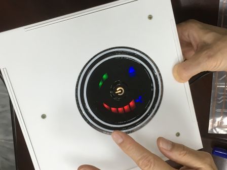
The circuits are produced on a relatively thick thermo-plastic sheet, either PET or polycarbonate, using screen-printing with silver paste. The circuit manufacturing process is the same as the process for thick film printed circuits produced with conductive inks. Single- and double-sided circuits with through holes are available. The circuits have almost no flexibility when the base thickness exceeds 100µm, but they can soften when heated to a temperature of 120°C. The soft circuit is then placed in a forming die using a little pressure, where the circuit forms to the shape of the housing device. Once the circuit cools down in the forming die set, it becomes a rigid 3-D structure. It is neither a rigid circuit board nor a flexible circuit. The construction has both electrical circuit and mechanical framing. The photo below shows the front side of a formed circuit applied to a switching panel.

A picture is worth a thousand words, but not in this case. You have to touch the circuit to appreciate its structure. The panel’s surface is not flat; it has several bumps and dimples inside the circle. A double-sided silver ink circuit with via holes was built on the opposite side using a screen-printing process. Many lighting components including chip shape LEDs were mounted on the circuit with conductive glue.
The idea behind the technology is not new. I remember similar technologies developed during the 1990s, and throughout the last couple of decades, various 3-D molded circuit technologies were developed based on the same idea. None of them were successful in commercial volume applications due to the low reliability of copper-based conductors. The corners and edges of the metallic copper conductors could easily crack during bending and molding of the circuits.
This Taiwanese circuit manufacturer did not use a new or unique technology to form the circuits, but did change the materials. They introduced a fine screen-printing process using several new ink materials to produce a more reliable conductor. The new inks have higher flexibilities compared with metallic copper, so the circuit is more reliable during forming. At this time, they can’t guarantee its reliability, so they prepared a design guide for the formed circuit to eliminate mechanical failures during manufacturing and assembling. The new circuit system cleared significant technical barriers for consumer applications.
This could be a breakthrough. More to come.
Dominique K. Numakura, This email address is being protected from spambots. You need JavaScript enabled to view it.
DKN Research, www.dknresearch.com
DKN Research Newsletter #1912, April 28th, 2019 (English Edition) (Micro Electronics & Packaging) This email address is being protected from spambots. You need JavaScript enabled to view it., www.dknresearch.com
*To view the newsletter archives, click here.
Headlines of the Week
1. Rohm (Major device manufacturer in Japan) developed a new AC/DC convertor IC “BM2SCQ12xT-LBZ” for power devices.
2. Canon (Major electronics company in Japan) developed a new CMOS sensor for monitoring cameras. It works under sever circumstances up to 120 degree C.
3. Nidec (Major motor manufacturer in Japan) agreed to buy a subsidiary company OEA from Omron to strengthen the business of automobile devices.
4. Tohoku University (Japan) co-developed a new n-type mixed conductor. It is stable at high temperature. It could be valuable to increase the performances of fuel cell batteries.
5. Sumitomo Corp. (Major trading company in Japan) started a subcontracting business of silicon base photonics devices with JSC (Japan Semiconductor Corp.).
6. Ilica Technologies (Battery manufacturer in U.K.) unveiled a new all-solid state battery “Stereax M5o” for in-plant use of the medical devices. It can be millimeter size.
7. Panasonic (Major electronics company in Japan) agreed with Rohm, major device manufacturer in Japan to sell several semiconductor (transistors and diodes) businesses.
8. TDK (Major device manufacturer in Japan) demonstrated the 1kW class wireless power supply system for unmanned vehicles in plant use. Some models are already in commercial use.
9. Kyoto University (Japan) discovered a photo catalyist to generate hydrogen using infrared light (wave length: 1100nm).
10. Murata (Major device manufacturer in Japan) recorded its highest revenue (1.5750 trillion yen) in 2018, a 14.8% increase from previous year. Profit increased 63.4%.
11. DISCO (Major semiconductor equipment manufacturer in Japan) will invest 17.5 billion yen to build a new manufacturing plant in Nagano Plant. It will be ten story building. Floor size: 132,000 square meters.


