Achieving Fine Lines and Spaces Using MSAP
A method to form fine-line circuits on organic substrates using traditional plating equipment.
These technological offerings of today and tomorrow are only possible with advances in the design of electronic components and printed circuit boards and the manufacturing processes required to decrease size, increase component density, and increase signal speeds, while maintaining high yields and competitive costs. This article reviews the historical subtractive print-and-etch method of producing an HDI PCB and discusses the MSAP process as a method to enhance HDI PCB capabilities.
Traditionally, HDI PCB circuit formation was produced using subtractive print-and-etch processing. The simplest form of this process begins with an outer foil layer of approximately 12 to 18µm in thickness into which blind vias are laser or mechanically drilled. The panels are then desmeared, either through a plasma or chemical desmear or a combination of both, to clean any resin residues from the target pad and impart some topography to the via walls for adhesion of subsequent deposits. The panels are then processed through a primary metallization process such as electroless copper, carbon-based direct metallization, or conductive polymer to make the via walls initially conductive, followed by a flash plating of 2 to 4µm of electrolytic copper.
After flash plating with electrolytic copper, the panels are processed through via filling electrolytic copper in panel plating mode. Copper via filling solutions are chemistries formulated to preferentially copper-plate microvias full, while minimizing buildup of surface copper. In this step, typically 20µm of surface copper are added to the existing 3µm of flash copper and 18µm of copper foil. The plated panels are then tented and etched with dry film to develop the circuit pattern. The exposed copper (~40µm) is etched away using conventional cupric chloride etchants to define the circuitry. Multiple layers are then built up using conventional materials and lamination processes, and the subtractive print-and-etch sequence is repeated.

Figure 1. Subtractive print and etch processing.
Conventional print-and-etch processing is limited in terms of minimum line width and spacing due to the tendency of the etching solutions to etch equally in all directions. This results in traces with trapezoidal profiles which become detrimental to product performance as line widths decrease (FIGURE 2). Defined and consistent line profiles with controlled impedance are critical in fine-line applications. Conventional print-and-etch processing is generally limited to line widths and spacing down to approximately 60 to 100µm, permitting single trace routing with pad pitches of 0.5mm (FIGURE 3).

Figure 2. Trace profile after etching.

Figure 3. Pad pitch and trace routing with subtractive print-and-etch.
Further miniaturization and increased functionality of electronic devices continued driving advances in conventional print-and-etch processing to prolong the life of this process technology and extend the capabilities to finer lines and spacings and smaller structures. From these advances arose processing technologies such as any-layer or everylayer printing and etching and advanced tenting processing (ATP). Enablers for these processes included improved laser drilling equipment, reduced copper thickness clad laminate, surface treatment for copper prior to laser drilling, and via fill copper plating processes.
Improvements in CO2 and UV lasers permitted more consistent drilling of high-quality blind microvias of smaller dimensions with improved via wall shape, even in the presence of glass webbing, less target pad damage, less target pad residues, and less splatter around the rim of the microvia. High-quality copper foils with reduced thicknesses ultimately result in less copper etch burden during circuit formation. Developments in surface treatment chemistries for copper prior to laser drilling improved consistency of laser energy absorption for more predictable, higher-quality drilling. Advances in via-fill electrolytic copper plating provided faster, more efficient via filling, while minimizing buildup of surface copper, again reducing the final copper etch burden. Finally, adoption and implementation of vertical continuous plating (VCP) equipment versus hoist systems dramatically improved consistency and thickness distribution of the copper plating processes.
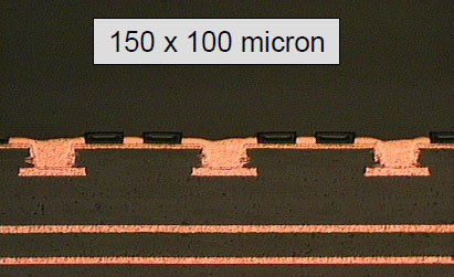
Figure 4. Typical print-and-etch microvias.
Anylayer print-and-etch and ATP are very similar to conventional subtractive processing (FIGURE 5). Several important differences in these processes versus the conventional subtractive print-and-etch process facilitate reduced line widths and spacing. Anylayer and ATP processing use no plated through-holes. Connections between layers are accomplished via stacked or staggered microvias. This eliminates the typical requirement for 25µm minimum of plated copper in the center of a through-hole, which can result in the need to plate upwards of 30µm of copper on the panel surface to meet specifications.

Figure 5. Subtractive print and etch processing.

Figure 6. Typical anylayer build.
In the absence of through-holes, electrolytic copper chemistries can be used that are designed specifically for preferential filling of blind microvias, while minimizing the buildup of surface copper. Microvias up to approximately 100µm in diameter and 75µm deep can be reliably filled with copper, while restricting the surface copper thickness to approximately 12µm. These chemistries operate off the voltage potential differences between the tops and the depths of the microvias and the selective adsorption of additives such as plating rate suppressors and plating rate accelerators under these conditions. The result is fast bottom-up filling of the microvias with copper and suppression of copper deposition on the surface (FIGURE 7).
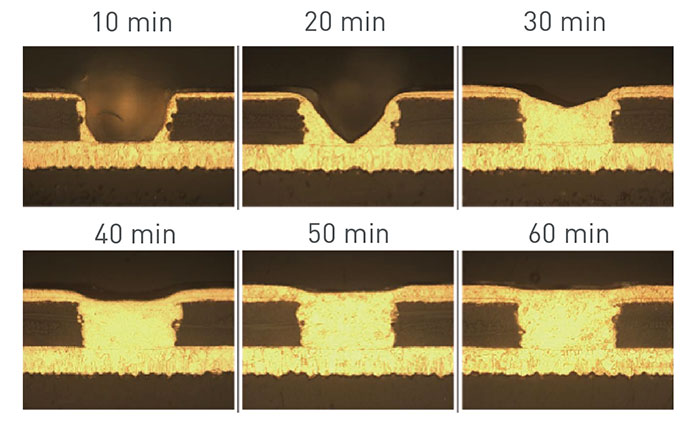
Figure 7. Preferential bottom-up filling.
The result of these changes and improvements is the overall copper thickness to final etch is reduced from approximately 40µm to approximately 27µm. This permits the line width and spacing to be reduced to approximately 40µm, in some cases 35µm with pad pitches of 0.4mm (FIGURE 8).
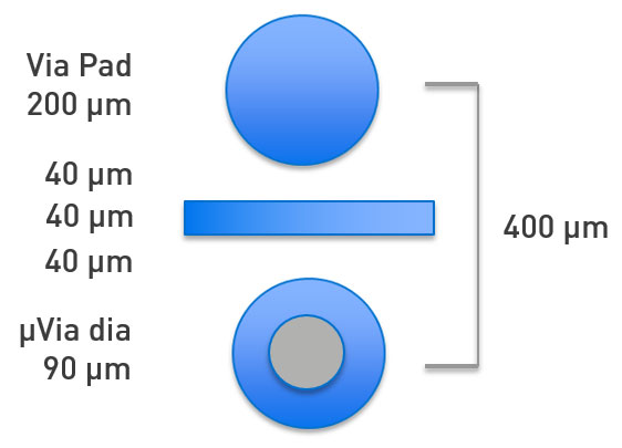
Figure 8. Anylayer pad spacing and line routing.
MSAP
Although considerable reductions in line widths and spacings have been accomplished through advancements in standard subtractive print-and-etch processing, further miniaturization necessitates thinner substrates and line widths and spacings too fine for the capabilities of subtractive print-and-etch processing with standard buildup materials.
The IC substrate industry has an established history with processes capable
of producing smaller features and fine high-resolution lines and spacings on inorganic substrates such as silicon using semiadditive processing (SAP). SAP processing uses ultra-thin base layers of copper deposited via PVD, CVD, or electroless copper deposition over the entire substrate surface, which are then laminated with photoresist, imaged using direct laser imaging and electrolytic copper pattern plated. The resist is then stripped, and the substrate is differential- or flash-etched to form the circuitry. The technology, though very capable, is prohibitively costly for use in the arena of 20 to 30µm line widths and spacings on organic substrates.
This arena is sometimes called substrate-like panels. In this area, there is a convergence of technologies where the adoption of IC substrate-like manufacturing processes is necessary to stretch the capabilities of the lower-cost organic substrate, while maintaining the desirable characteristics such as large-format, lower-cost organic panels and standard high-production plating equipment (FIGURE 9). The process developed for the manufacturing of substrate-like panels has been termed MSAP, or modified semiadditive processing. The characteristics associated with this type of processing include:
- Line widths and spacing of 30µm/30µm → 20µm/20µm.
- Pad pitches of 0.35mm.
- Double trace routing between pads.
- Blind microvias of 55 to 65µm in diameter and 0.6 to 1.0 aspect ratio.
- Consistent trace profiles for controlled impedance.
- Low-cost organic substrate.
- Low-cost mass-production-capable processing.

Figure 9. Convergence of technologies.

Figure 10. MSAP pad spacing and line routing.
The main concept behind MSAP processing (FIGURE 11) is to minimize the amount of copper buildup at each stage of the process, with the ultimate goal of minimizing the final amount of copper required to etch for circuit formation. This is referred to as the copper budget. FIGURE 12 illustrates the typical copper budget for several variations of the MSAP process. The numbers in black represent copper added in the various process steps, while the red numbers represent copper subtraction from various surface treatments or microetches.

Figure 11. MSAP processing.
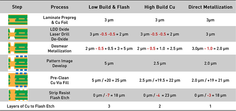
Figure 12. MSAP copper budget.
The typical MSAP process flow (see Figure 11) begins with an organic substrate clad with a very thin copper foil of approximately 3µm in thickness. In the past, very thin copper foils were not readily available, so thicker foils needed to be chemically reduced via horizontal etching. As the technology developed, however, foil suppliers now provide 1 to 5 µm starting foils necessary for MSAP processing at competitive pricing.
Microvias are then laser-drilled and the panels desmeared, either through a plasma or chemical desmear or a combination of both, to clean any resin residues from the target pad and impart some topography to the via walls for adhesion of subsequent deposits. The panels are processed through a primary metallization process such as electroless copper, carbon-based direct metallization, or conductive polymer to make the via walls initially conductive, followed by a flash plating of 2 to 4µm of electrolytic copper. In some instances, rather than flash plating after primary metallization, fabricators utilizing electroless copper will increase the electroless copper thickness to approximately 1.0 to 1.2µm and omit the electrolytic copper flash to save on additional electrolytic copper plating.
Panel plate via filling is not done in MSAP, as this adds undesirable plated copper thickness that must be final etched, thus detrimentally affecting fine-line trace profiles and process capability. The panels are imaged using laser direct imaging and pattern-plated with approximately 18 to 20µm of copper. The pattern plating is done both to fill the microvias completely with copper and build the copper traces to the required height. Advancements in electrolytic via fill copper chemistries have improved the speed and efficiencies of via filling, while minimizing the amount of surface copper. At the same time, they have improved the overall profile of the traces in terms of flatness, both within the structure as well as across a large panel, permitting mass production of precise structures.
After plating, the resist is stripped and a differential or flash etch is done to form the final circuitry. Because pains were taken to control the amount of copper deposited throughout the process, a typical total of only 2 to 3µm of copper is removed in the flash etch. This minimal copper etching preserves the profile of the circuit traces, permitting the production of finer lines (FIGURE 13).
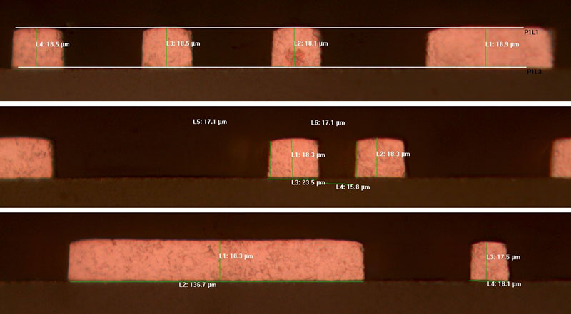
Figure 13. Trace profile after MSAP processing.
Multiple layers are then built up using prepregs tailored to MSAP processing. These prepreg layers are much thinner to accommodate smaller microvias and the desire for reduced thickness board profiles. Dielectric thicknesses can be as low as 40µm. They must also be more dimensionally stable in the z-direction under thermal excursions to reduce the mechanical stresses placed upon the plated microvias, whose interconnect contacts areas are greatly reduced when reducing feature sizes. The reduced contact areas decrease the absolute load required to pull the structure apart.
Which Process to Use?
The choice of whether to use MSAP or any of the other processes outlined above to build a product will ultimately depend on the board design, application, and the need for finer-line widths and spacings balanced with the relatively higher costs of MSAP processing (equipment and materials) versus conventional subtractive print-and-etch. FIGURE 14 provides a general overview of the various processes discussed and where they fit, as driven by line width and spacing requirements. In general, conventional subtractive print-and-etch can be used for line widths and spacings down to approximately 60µm/60µm. Use of anylayer processing extends subtractive print-and-etch down to 40µm/40µm line widths and spacings and ATP to 35µm/35µm. Further reduction in line widths and spacings would favor MSAP processing with capabilities as low as 20µm/20µm.
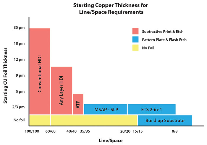
Figure 14. Process capabilities.
Summary
The desire for greater device functionality, connectivity and speed in small, portable devices at affordable prices continues to drive miniaturization of electronics, necessitating reductions in the sizes of features such as microvias, line widths, line spacings, and dielectric thicknesses. Reductions in line widths and spacings and the applications in which they are used require critical control of trace profiles for optimum performance. FIGURE 15 details these reductions to scale.
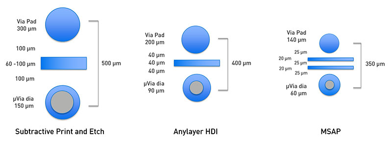
Figure 15. The evolution of interconnection to MSAP.
The evolution of conventional subtractive print-and-etch processes has extended the capabilities of this type of processing to the level of 35µm/35µm line width and spacing. Further reductions required adoption of various SAP manufacturing processes commonly used in the IC substrate industry, including LDI resists and imaging, improved laser drilling, extremely thin copper foils, via fill pattern plating, and flash etching into a process called MSAP.
MSAP provides a reliable, cost-effective manufacturing process for the production of fine-line HDI on organic substrates down to 20µm/20µm line widths and spacing using conventional, high-volume plating equipment such as vertical continuous platers. MSAP provides high yields on large-format boards, enabling control of manufacturing costs on substrate-like panels.
Bibliography
- T. Rapala-Virtaner, E. Helminen and T. Jokela, “Next-Generation Ultra-Thin HDI PCB Manufacturing Challenges,” The PCB Magazine, May 2015.
- M. Gantz, “mSAP: The New PCB Manufacturing Imperative for 5G Smartphones,” Electronic Design, electronicdesign.com/industrial-automation/msap-new-pcb-manufacturing-imperative-5g-smartphones, Oct. 23, 2017.
- J. Rasmussen, A. Lachowicz, D. Isik and H. Verbunt, “Microvia Filling: A Challenge for Process Quality,” OnBoard Technology, April 2006.
is applications manager, metallization at MacDermid Enthone Electronics Solutions; This email address is being protected from spambots. You need JavaScript enabled to view it.. is technical marketing specialist, MacDermid Enthone Electronics Solutions; This email address is being protected from spambots. You need JavaScript enabled to view it..


