Guidelines for Improving PCB Design Manufacturability
Best practices for daily routines.
Completing the development stage of a printed circuit board (PCB) design and handing it to manufacturing should be the proverbial passing of the torch, the moment that signals the final stages of a design’s lifecycle. But what happens when the PCB design is flawed or missing a necessary component? What happens if incomplete files are released to production, resulting in a nonconforming PCB, or the PCBs are degraded in the field? These common missteps force engineers to either backtrack the design layout itself or the documentation they painstakingly worked to produce, with either scenario prompting extensive rework or delay.
Unfortunately, these scenarios are all too common for many engineers.
Navigating the post-design stage can be tricky, and it’s easy to unintentionally create stumbling blocks in the process. If the proper methods for maintaining PCB design data aren’t utilized or structured in a way that can be easily interpreted by production, engineers run the risk of compromising the entire design’s manufacturability. Mistakes made during the actual development process can have similarly detrimental effects.
Is there a general rule of thumb when it comes to maneuvering the development and production stages of PCB design and making sure every specification is well documented? The good news is there are practical, applicable guidelines to follow for transitioning into the fabrication, assembly and production stages of a design.
Let’s start with the foundation, the design process. What’s the key to designing a board that’s realistic on paper and manufacturable, functional and reliable in physical form? When starting a design, it’s easy to leave the PCB design guidelines as an afterthought, as engineers spend most of their time focusing on the circuit design and component selections. But at the end of the day, not providing ample time and focused effort on the PCB can lead to a design that translates poorly from the digital domain to physical reality, and could ultimately become troublesome for the manufacturer to fabricate.
Fine-tuning component placement. The component placement stage of the PCB layout process is both an art and a science, requiring strategic consideration about the prime real estate available on a board. And while this process can be challenging, how components are placed will determine how easy the board is to manufacture, in addition to how well it meets the original design requirements. Several specific guidelines include:
- Orientation. Orient similar components in the same direction, as this will help with an efficient and error-free soldering process (FIGURE 1).
- Placement. Avoid placing components on the solder side of a board that would rest behind plated through-hole (PTH) components.
- Organization. Place all surface mount (SMT) components on the same side of the board, and all PTH components on the top side of the board to minimize the number of assembly steps (FIGURE 2).
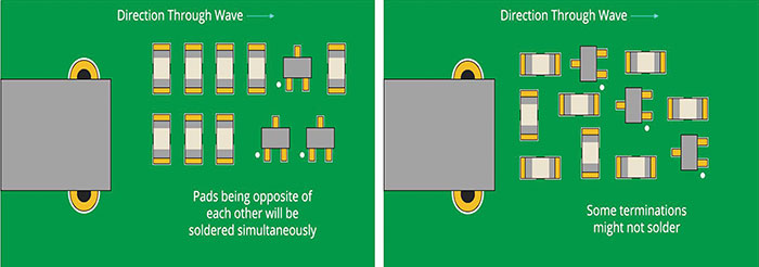
Figure 1. Good orientation for chip components (left) and poor orientation for chip components (right).
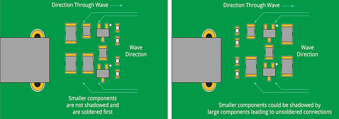
Figure 2. Good placement for components (left) and poor placement for components (right).
One final PCB design guideline to keep in mind: when using mixed-technology components (through-hole and surface mount components), manufacturers might require an extra process to assemble the board, which will add to the overall costs.
Power, ground and signal trace placement. Once the components have been situated on a board, the next step is to route the power, ground and signal traces to ensure the signals have a clear and distinct path of travel. Here are some important things to keep in mind for this stage of the layout process:
It’s always recommended to have the power and ground planes internal to the board, symmetrical and centered. This will help prevent the board from bending, which will also affect whether the components are properly positioned. To power the integrated circuits (ICs), use common rails for each supply, ensure there are solid and wide traces, and also avoid daisy-chaining power lines from part to part.
Next up is connecting the signal traces to match the schematic guidelines. Place traces as shortly and directly as possible between components. If the component placement forces a horizontal trace routing on one side of the board, then place traces vertically on the opposite side.
Designs typically require different nets that will carry a wide range of currents, which will dictate the required net width. With this basic requirement in mind, provide a 0.010" width for low current analog and digital signals; when traces carry more than 0.3A, it should be wider.
Keeping board parts separate. Most designers have likely experienced how large voltage in power circuits and current spikes can interfere with low voltage and current control circuits. To minimize this interference, follow these guidelines:
- Separation. Keep the power ground and control ground separate for each power supply stage. If tying them together is necessary, make sure it’s toward the end of the supply path.
- Placement. If the ground plane is placed in the middle layer, be sure to place a small impedance path to reduce the risk of any power circuit interference and help protect the control signals. The same guideline can be followed to keep the digital and analog ground separate (FIGURE 3).
- Coupling. To reduce capacitive coupling due to the placement of a large ground plane and the lines routed above and under it, have the analog ground crossed only by analog lines.
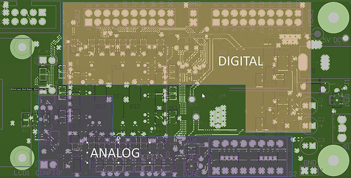
Figure 3. Example of component separation (digital and analog).
Avoiding high heat circuits. At some point in their careers, most engineers have experienced degraded circuit performance and board damage due to heating. This problem afflicts many boards when heat dissipation isn’t taken into consideration. Here are some essential guidelines to consider to help combat these issues:
The first step is to start considering which components will dissipate the most heat on the board. This can be accomplished by first finding the thermal resistance ratings in the component’s datasheet, and then following the recommended guidelines to divert the heat being produced. Of course, heat sinks and cooling fans can be added to keep component temperatures down. It is also important to remember to keep critical components away from any high heat sources.
Adding thermal reliefs can be incredibly useful to produce a manufacturable board, and they are critical for the wave soldering application on high copper content assemblies and multilayer boards (FIGURE 4). Because it can be difficult to maintain process temperatures, utilize thermal reliefs on through-hole components to make the soldering process as easy as possible by slowing the rate of heat sinking through the component plates.
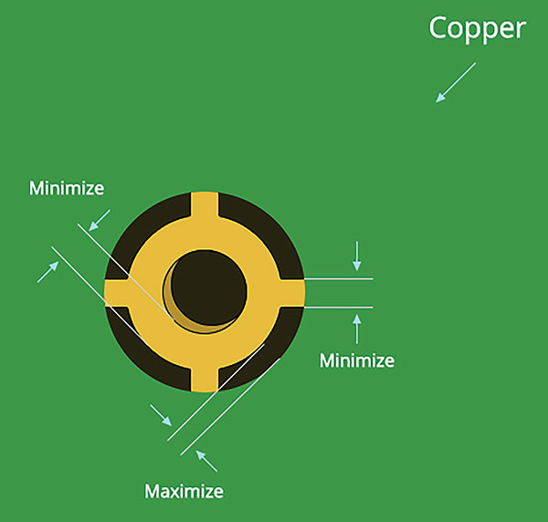
Figure 4. Typical thermal relief pattern.
As a general guideline, always use a thermal relief pattern for any via or hole that is connected to a ground or power plane. In addition to thermal reliefs, designers can also add teardrops where traces join pads to provide additional copper and metal support. This will help reduce mechanical and thermal stress.
Authenticating the work. Scrambling to fit the remaining pieces of the design together in preparation for manufacturing can be overwhelming as the end of a project nears. Nevertheless, double- and triple-checking the work for any potential errors at this stage can mean the difference between a manufacturing success or failure.
To improve the quality control process, always start with the electrical rules check (ERC) and design rules check (DRC) to verify all established constraints have been met. With these two systems, it’s easy to enforce gap widths, trace widths, common manufacturing setups, high-speed requirements and short circuits.
When both the ERC and DRC have produced error-free results, check the routing of every signal and confirm nothing has been missed by running through the schematic one wire at a time. This also ensures the PCB layout matches the schematic by utilizing the design tool’s probing and masking features.
Transitioning to production. By sticking to these guidelines, engineers can confidently design functional and manufacturable boards that meet every fabrication and assembly requirement. Good PCB design practices are crucial for success, and these design rules reinforce continual improvement in every stage of the design process. That said, the design journey doesn’t stop there. The next (and most critical) step of the design project lifecycle is the transition to manufacturing. While this phase can be tedious, demanding time and attention to detail, both the engineer and fabricator are grateful when this stage is managed properly.
Communication is key, and there’s a reason why this notion persists. It applies to our personal and professional environments, and everything in between. So why would it be any less relevant to something as detail-oriented as PCB design and manufacturing?
Many of today’s design processes lack transparency when transitioning from one stage to the other, leaving the door wide open for misinformation, mismanaged workflows, missing documentation, incorrect parts and a myriad of other issues that can compromise manufacturability. That’s a tough position for any engineer or design team to be in, and the pressure to fix each respective problem in a timely fashion without exerting the budget can be immense. So how can you prevent your design from being rejected? Knowing what to do in the pre-production stage helps design teams avoid complications in the post-design stage. Poor management practices not only have immediate ramifications for design teams, but also trigger a chain reaction that reverberates down the supply chain.
Submitting documentation content. Transitioning from design completion to manufacturing is seldom a straightforward path, but it’s crucial for design teams to have all their ducks in a row when submitting their final product and accompanying documentation over to production. If the documentation package falls short in any way, it can set back the entire production process. Knowing how to avoid these complications altogether is key for a smooth, painless transition to manufacturing.
One major error that raises an immediate red flag for any manufacturer is a missing piece of documentation or sets of missing documentation in the design files. Incomplete or inconsistent production documentation can bring the manufacturing process to a complete standstill. Having to backtrack the entire documentation process, correct existing errors and ensure those changes are communicated to the manufacturer is time-consuming and costly. When assembling a documentation package, here are a few things to keep in mind:
- When using a PCB design tool that requires a manual generation of output documentation, pay close attention to the output files and keep them organized in a single repository.
- Confirm with the manufacturer exactly what files it requires and in what format (Gerber, ODB++, IPC-2581, etc.) before sending anything.
- Never send the manufacturer a single, internal CAD file assuming it has the necessary software to read it.
To put it simply, a complete PCB documentation package should contain all the files required by the manufacturer, organized in a file format and structure that is easily interpreted without any guesswork. Any redundant or errant files found by the manufacturer will only add delays to the production process.
Ambiguous class types. While Class 2 is the industry standard for PCB documentation, the master drawing will change drastically if the design was created using a different class (i.e., Class 1 or Class 3). Because of this, it’s important to clarify which class is being used with the following guidelines:
- So the manufacturer does not assume a standard Class 2 process is required, call out the preferred build standard of whichever class is needed on both the PCB fabrication and assembly drawings.
- In the event there are varied process preferences for specific components, indicate that they require different treatment than what the assembly drawing specifies (e.g., a Class 2 assembly with a Class 3 hole fill requirement).
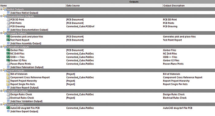
Figure 5. Complete documentation data package (output job files).
Indicating the class requirement in the drawing package will ensure that the PCB gets processed properly, while also assisting during the technical review process. This critical piece of information will ultimately permit the manufacturer to provide the most accurate quote possible, while also successfully manufacturing the board.
Missing solder specifications. In the past, manufacturers weren’t overly concerned about whether a PCB needed to be lead-free. However, with the Restriction of Hazardous Substances (RoHS), PCB manufacturers are now required to support a variety of solder and flux combinations. To properly document a design to meet RoHS requirements, keep in mind the following:
- Any business that sells applicable electronic products to RoHS countries must comply with this directive and indicate compliance in documentation notes.
- While RoHS might be the standard now rather than the exception, it’s important to indicate on the documentation packages where RoHS specifications are not needed, using a non-RoHS designator.
RoHS compliance is here to stay. To stay ahead of the game, engineers should ensure proper documentation of the PCB specifications with RoHS or non-RoHS-specific designators as needed, to avoid delaying production.
Missing ITAR requirements. For US-based companies, financial and legal issues associated with having a design sent overseas and handled by a non-US person is something that needs to be taken seriously and documented thoroughly. Keep these criteria in mind for documenting International Traffic in Arms Regulations (ITAR) requirements:
- As more aspects of the PCB design industry supply chain become outsourced, engineers must specify ITAR requirements in their documentation to ensure their data packages are handled properly.
- Ensure ITAR requirements are documented in the correct location. Some manufacturers receive ITAR specs on purchase orders instead of the fabrication and assembly drawings.
By carefully documenting ITAR requirements, design teams can avoid putting both themselves and the manufacturer at risk for accidentally mishandling sensitive ITAR data.
Missing layer sequences. The specific arrangement of the layer stackup is a critical component for an electronic design, especially high-speed digital designs requiring matched impedance transmission lines. Here are a few things to be aware of when documenting layer sequences:
- Layer numbers should be indicated in the copper image, with the logical number placed in each layer. Starting from the top, use 1 for top layer, 2 for inner 1, 3 for inner 2 and so forth. If this indication method is used, position the numbers in a way where they won’t overlap (FIGURE 6).
- Include in the assembly and fabrication drawing a clear stackup drawing that includes all copper layers, solder mask, overlay layers and any additional layers in the correct sequence and with the corresponding correct data file names.
- Name each layer file in a manner that clearly shows the correct sequence (e.g., Top, Mid1, Mid2, and so on).
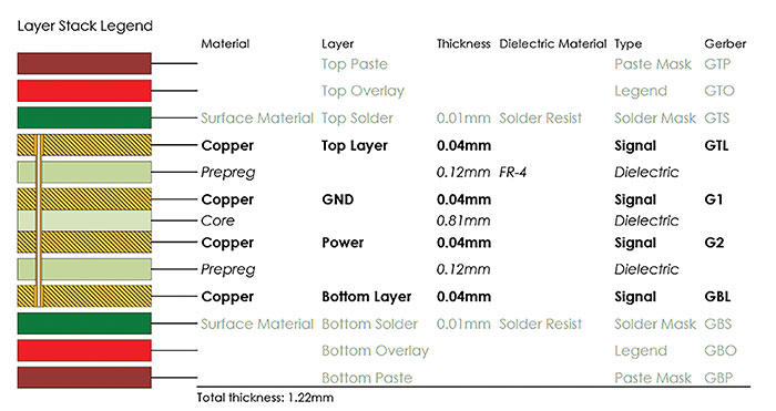
Figure 6. Ideal PCB drawing layer stackup legend with Gerber file names.
Excluding layer sequences from a documentation package can result in improperly functioning boards and resins, or other potential defects with a design. Adhering to the guidelines above gives engineers a solid foundation to effectively communicate their design intent to the manufacturer, giving both parties the green light to move forward in the production process.
The design process is never foolproof, and problems are likely to arise in one form or another. But knowing what to expect and how to mitigate these issues early on in the design process gives engineers the upper hand in what at times may seem like an uphill battle. Design teams that incorporate the above guidelines and best practices into their daily routines will reap several benefits, including transparent design objectives, organized workflows, conforming boards that meet all fabrication and assembly requirements, and complete documentation materials. Combined, all of these elements work synergistically to help engineers produce quality, manufacturable electronic designs every time.
is a senior technical marketing engineer at Altium (altium.com); This email address is being protected from spambots. You need JavaScript enabled to view it..


