Empirical Results of Fusing Tests
Slight current overloads result in unpredictably long fusing times.
In September 2015, Dr. Adam and I looked at the question of how big a trace needed to be in order to carry a current overload for a short period of time.1 The question asked in that article was
What if a trace normally carries a nominal current, but then, under catastrophic failure conditions, is subject to a severe overload? It may be necessary for the trace to be able to carry that overload for a short period of time – maybe one second or so – while the system shuts down in a controlled manner. A controlled shutdown may be necessary to prevent further system damage, or perhaps to prevent human injury. Then how big does a trace need to be?
We used a computer simulation tool called TRM2 to estimate the relationship between the size of an ideal trace, the current overload it is carrying, and the time it takes the trace to reach the melting temperature. This article reports on an empirical investigation into the same relationships on actual traces.
This type of empirical analysis would not have been possible without the cooperation of several people. In particular, I want to thank my longtime partner Dave Graves (now with Monsoon Solutions in Bellevue, WA) for helping prepare the final artwork for the test board. A special thanks to Prototron Circuits (of Redmond, WA), which provided the test boards. And my collaborator on trace thermal issues, Johannes Adam (Leimen, Germany), continues to be a great help in evaluating results.
We can group trace thermal overload situations into two broad categories:
- Strong overload, in which the current is much higher than the trace can handle, resulting in fusing times within 0.0 to about 5.0 sec. or so. This case is relevant for the question raised in the referenced article.
- Slight overload, in which the current is a little higher than the trace can handle, resulting in fusing times ranging from minutes to hours. This case is relevant for a trace, carrying high current, or relies on external aids for supplemental cooling – such as forced air or a buried heat sink. If the supplement aid is compromised, the trace temperature may increase to the point at which thermal “runaway” is inevitable.
Problems Predicting Fusing
Simulation programs typically assume the materials (in this case the copper trace and the board dielectric material) are homogeneous, and the conditions are predictable. This is not necessarily true under fusing conditions. Four major components of the fusing environment need to be considered:
1. Heating. Traces heat by I2R power dissipation in the trace. Power is also given by v*i (voltage times current.) Under experimental conditions, both voltage and current can be measured with fairly high precision, so this is typically not too big a problem. The trace resistance can be found by dividing voltage by current (v/i). The temperature change is given by the same formula found in theIPC test procedure 2.5.4.1:
![]() [Eq. 1]
[Eq. 1]
where:
ΔT = change in temperature from ambient (ref) (oC)
α = thermal coefficient of resistivity of copper (1/oC)
Rt = resistance at the temperature under test Ω
Rref = resistance at the reference temperature Ω
It should be noted this leads to the average temperature of the trace, which, because of thermal gradients (especially at the ends of the trace), is not the maximum temperature anywhere along the trace.
Computer models typically assume α is either a constant or that it changes linearly with temperature, and also that resistance changes linearly with α. As traces heat to relatively high temperatures, neither of these assumptions may continue to be true.
2. Cooling. A PCB trace typically cools primarily by conduction through the dielectric and secondarily by convection and radiation into the air. A stable temperature is reached when heating equals cooling. Computer models are reasonably
good at handling the conductive cooling, as long as the thermal properties of the material are known and predictable (i.e., as long as the material properties don’t change.) If the thermal properties are not predictable, then the computer model can no longer provide reliable results.
Convection and radiation are typically handled in TRM by a factor called HTC, or heat transfer coefficient. The values of HTC are reasonably well understood for temperature changes in the range of up to 100˚C or so. But they are very difficult to predict if there are hot spots or for a temperature range of 1,000˚C, especially if the timing associated with that range of temperature is uncertain.
3. Trace (copper) properties. There are typically two types of copper on PCBs: There is the copper foil that is bonded to the dielectric material in the supply process and copper plating applied by the board fabricator (typically on the outerlayers). Since “copper is copper,” it is tempting to think a model could consider copper traces to be homogeneous, but let’s take a closer look.
Copper foil is fabricated under well-controlled conditions. There might be a tolerance on the foil thickness, but otherwise, it should be fairly homogeneous. On the other hand, there might be microscopic contamination that exists at places under the foil that happens during the bonding process. If these change the heat transfer characteristics between the foil and dielectric, then unpredictable thermal hotspots might develop at these points.
There is also a lack of understanding in the literature on how the resistivity and α vary (if, in fact they do) between copper foil and plated copper. (Look for a future article on this topic.)
The copper plating process is inherently less well-controlled. Plating can (and does) vary in thickness on the board (and therefore possibly along a trace), and there are more opportunities for contamination to occur. Again, these can lead to hotspots along a trace.
Finally, final trace dimensions are defined by a photo-etch process. There can be small variations in trace width along a trace. Narrower places along a trace heat more quickly.
4. Dielectric properties. Dielectric materials, at least from reliable manufacturers, are quite homogeneous. However, typical materials (such as FR-4) have three parameters of interest here:
Tg. Glass transition temperature (Tg) is the temperature region where the polymer transitions from a hard, glassy material to a soft, rubbery material. This results in dimensional changes and some change in thermal conductivity. This changes the way in which the dielectric is able to conduct heat away from the trace. It is reversible. A typical specification for Tg is around 170˚C.
Td. The thermal decomposition temperature is the temperature at which weight loss begins to occur.4 Thermal decomposition is typically specified around 300˚ to 350˚C. Thermal decomposition will change the ability of the dielectric to carry heat away from the trace. It is irreversible.
In addition, if the board begins to delaminate, all bets are off, and the trace will begin to heat uncontrollably and probably fairly rapidly. The material used in this evaluation had a “thermal resistance” (time to delamination) specified as:
T = 260˚C >60 min.
T = 288˚C >20 min.
The Fusing Process
The fusing process can be subdivided into two broadly defined categories (as defined above), strong overload (leading to rapid fusing), and long-term, or slight, overload (leading to slow fusing that might take minutes or hours).
If we submit a trace to a strong overload (relatively large current), the temperature rises quickly to the point where the weakest spot on the trace melts. The weakest spot on the trace is unpredictable and will typically vary from trace to trace. The melting process will be rapid, particularly because there is “positive” feedback. That is, the rising current results in rising temperature, which raises that resistance, which increases the temperature, which raises the resistance.
If we apply just enough current to ultimately cause the trace to melt, the failure process goes through several separate steps. First, the trace temperature will rise to a plateau and seem to level off. If this is near Tg, the temperature will slowly increase until it gets in the vicinity of the delamination temperature. The temperature will start increasing a little faster until it gets near Td. At that point the temperature really accelerates until the trace melts at the weakest spot along the trace. The entire process can take from tens of seconds to hours.
If we plot trace temperature against time, we can’t necessarily identify the precise times at which these transitions occur. They will occur at points within, or perhaps underneath, the copper trace itself and by their very nature are “point” phenomena. (Remember, the calculated trace temperature is an average over the entire trace length, not the temperature at the hottest point.)
Empirical Results
As a result of Prototron’s generosity, several boards were available for evaluation. The test equipment available included a constant current power supply and a portable oscilloscope. The maximum current capacity of the power supply was 10A, which limited the investigation to smaller traces. Separate evaluations suggested the accuracy of the power supply and of the scope were within 2 or 3%.
Traces were 6" long and varied in trace width from 15 mils to 27 mils. Most were 0.5 oz. foil plated over with 1.0 oz. copper, although there was one board that was 0.5 oz. foil only. Separate microsection measurements showed trace widths were well controlled, but the total foil plus plating thickness could vary between 1.9 mils and 2.6 mils, worst case. This article will report on three cases.
Case A (fast fusing). A 15 mil wide, 0.5 oz. trace was subjected to a sudden current of 6A. The trace fused in 2.75 sec. (FIGURE 1). The curve of voltage vs. time ramps in an almost straight line. Temperature lines are shown on the curve for reference. These are approximate; see note 5 for an explanation of how they were derived.
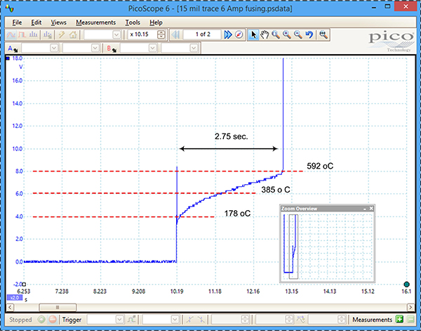
Figure 1. 15 mil wide, 0.5 oz. trace carrying 6A.
A video was taken of the trace fusing. The moment of fusing was somewhat underwhelming. Fusing occurred within one video frame (1/30th sec.)(FIGURE 2).There was no smoke and virtually no aroma. There was negligible damage to the board under and around the trace.
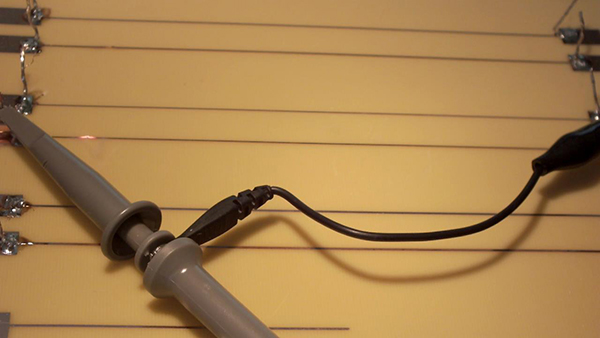
Figure 2. 15 mil wide, 0.5 oz. trace at the moment of fusing.
A thermal simulation of this trace calculated the fusing time at 4 sec. This is close and likely the fusing time had the trace and board been homogeneous. Results are partially predictable because the heating happens so quickly there is little opportunity for any cooling discontinuities to develop. This is evidenced by the lack of any visible damage to the board material. But as discussed above, inherent potential hot spots related to the copper can cause localized heating. The trace fuses at its weakest point, and that point is much hotter than the surrounding trace. There is no way to predict or explain why that particular point was the weakest point. The average temperature of the trace is still low when the trace fuses at its weakest point.
Case B (slow fusing). A 20 mil wide, 1.5 oz. trace was subjected to 8.5A. This trace, being 33% wider and three times thicker than the case above, took much longer, about 30 min., to fuse. The curve of voltage (and therefore temperature) vs. time is shown in FIGURE 3.
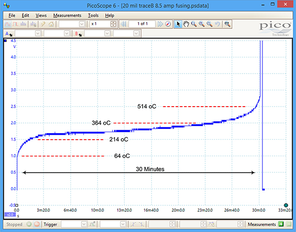
Figure 3. 20 mil wide, 1.5 oz. trace carrying 8.5A.
Here the curve tends to level out somewhere around maybe 250˚ or so and then starts a slow climb upward. As the temperature increases, the rate of increase also increases. Some people have described this as a thermal runaway. Once it starts, its progress is inevitable, unless the current is interrupted.
When this trace fused, the results were much more spectacular. FIGURE 4 illustrates the moment of fusing. First, the trace began to visibly glow about 35 sec. before fusing. It began smoking some 90 sec. before fusing. The aroma of burning material was in the air for perhaps 15 min. before fusing.
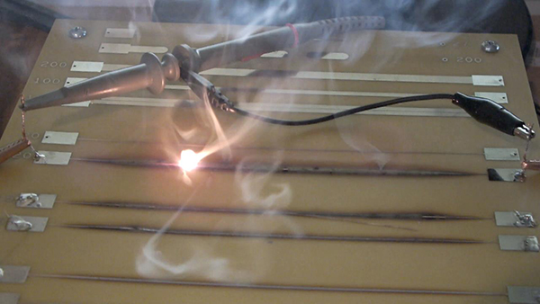
Figure 4. Moment of fusing for a 20 mil wide, 1.5 oz. trace carrying 8.5A.
Note in Figure 4 how smoke is being visibly ejected under pressure from several places along and under the trace. The board shows visible signs of heat damage, and closer inspection shows continuous areas of what appear to be bubbles (delamination) along the edges of the trace.
Other cases. The current required for the kind of “thermal runaway” described in Case B, above, is very trace-specific. This is because the discontinuities associated with each trace and each spot on the board are different. For example, FIGURE 5 and FIGURE 6 illustrate the same trace carrying 8.3A and 8.4A, respectively. (The 8.4A was applied 12 hr. after the 8.3A, permitting plenty of time for cooling between tests.) At 8.3A, the trace showed no signs of running away after 120 min. The same trace carrying 8.4A fused at 76 min. Another trace on another board with the same dimensions and carrying 8.5A showed no signs of runaway for over an hour, illustrating how there can be minor but important differences between traces and boards.
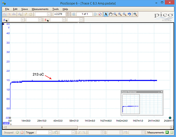
Figure 5. 20 mil 1.5 oz. trace carrying 8.3A showed no signs of runaway after 120 min.
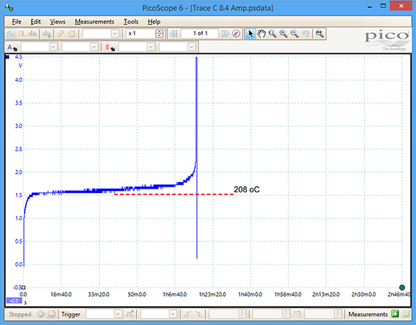
Figure 6. Same trace carrying 8.4A fused in 76 min.
Conclusions
The fusing time of a trace subjected to a heavy current overload (and fusing between 0.0 and maybe 5 sec.) is modestly predictable. Under these conditions there is negligible time for any cooling effects to kick in, and the board material properties remain constant. The trace fuses quickly at a specific point, and there is little damage to the surrounding board area, as well as little aroma associated with type of failure.
Slight current overloads result in unpredictably long fusing times (as long as hours). This type of overload might occur, for example, if a trace relies on supplemental cooling processes – say flowing air or an embedded heat sink – and that process degrades for any reason. The board material shows significant damage all along the trace, and smoke is apparent. Some smoke is ejected from under the trace under significant pressure. The trace may glow red hot for several seconds before it fuses.
There is heavy material damage under and around the trace. When the trace finally fuses, it does so along a small distance (not at a specific point), the copper seeming to “curl back” as it melts. The aroma of burning is pervasive.
Nominally identical traces have different currents where the slight overload, sometimes referred to as thermal runaway, will result in a fusing condition. This is because of unpredictable discontinuities in the board material and the copper composition.
Notes
1. Douglas G. Brooks and Johannes Adam, “PCB Fusing Currents,” PCD&F, September 2015.
2. TRM (Thermal Risk Management), developed by Dr. Johannes Adam, is the software tool used. See adam-research.com for more information regarding the tool and these types of simulations.
3. IPC-TM-650, Test Methods Manual, no. 2.5.4.1A, “Conductor Temperature Rise Due to Current Changes in Conductors,” August 1997.
4. IPC-TM-650, , “Decomposition Temperature (Td) of Laminate Material Using TGA,” April 2006.
5. Temperature reference lines in Figures 1, 3, 5, and 6 are estimated. The reference resistance (at 20˚C) was calculated using nominal trace geometry and a resistivity of 0.67µOhm-in. Resistance at temperature was calculated from v/i (Ohm’s law). The elevated temperature was then calculated using Equation 1 using the thermal coefficient of resistivity as 0.0039. Remember, these are average trace temperatures along the trace, not the peak temperature at any point.
is owner of UltraCAD Design, a PCB design service bureau and author of PCB Currents: How They Flow, How They React; This email address is being protected from spambots. You need JavaScript enabled to view it..


