The 5 Pillars of PCB Design Best Practices
Our newest column shares tips and tricks and lessons learned over 30 years in PCB design.
 With today's complex printed circuit board (PCB) designs challenging us at almost every stage of the design process, along with shortened project schedules and shrinking budgets, achieving success is no easy feat. Smaller component packages, faster signal edge rates or rise times, and increased design for manufacturing (DfM) challenges all make it difficult to achieve success and get product to market on time and under budget. The foundation for achieving success is understanding PCB design (the full design process) and mastering the power of today's EDA tools.
Even so, design teams can lose valuable time on unproductive tasks. Designers need a collaborative approach to electronic systems design that keeps them connected through all engineering disciplines and gives them best-in-class solutions to handle complexity across the entire PCB design process.
More specifically, we are experiencing heightened complexity in four key areas.
- Product complexity, including advanced packaging technologies, transmission speeds, multi-discipline co-design, component count and density, form-factor, and material technologies.
- Organizational complexity, including collaboration across engineering disciplines, collaboration across geographies, knowledge management, and workforce productivity and efficiency.
- Process complexity, including user-experience, integrated verification, heterogenous tool chains, system engineering, system decomposition and verification, and streamlined design to manufacturing.
- Supply chain complexity, including global supply shortages, contractor management and assessment, alternate supply, pricing volatility, risk assessment, and sourcing visibility and knowledge.
If you're a PCB designer, an electrical engineer, or someone else involved with printed circuit engineering looking to optimize the tools and processes you use throughout the full PCB design flow, you will want to follow this column series on PCB design best practices.

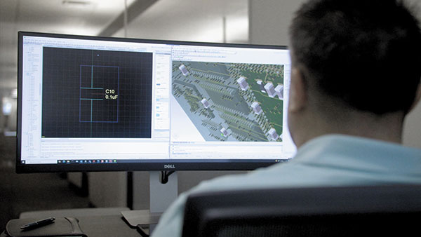
Figure 1. The foundation for success in PCB design involves both understanding the full design process and mastering the CAD tools.
Why am I sharing PCB design best practices? My objective is to share with you what I've learned over the past 30 years: tips and tricks and lessons learned regarding printed circuit design. I'll do that by breaking down PCB design best practices into five categories, or what I refer to as the five pillars.
- Digitally integrated and optimized: Under this pillar, I'll cover electromechanical co-design, design and manufacturing, library and data management, work-in-progress data management, and PLM integration.
- Engineering productivity and efficiency: Under this pillar, I'll cover automation (placement, route, and outputs), analog/digital/RF co-design, concurrent design (schematic and layout), design reuse, constraint driven design, and advanced design for both rigid-flex and high-density interconnect (HDI).
- Digital-prototype driven verification: Under this pillar, I'll cover shift-left approaches, specifically regarding the analysis and domain specialists.
- System-level model-based engineering: Under this pillar, I'll cover multi-board design, FPGA/PCB optimization, and IC/package/PCB co-design.
- Supply chain resilience: Under this pillar, I'll cover design for resilience, which really became a major issue to deal with as the pandemic caused significant negative impacts worldwide.
These pillars cover the full spectrum of printed circuit engineering and printed circuit board design, and as I cover each of them in this series month to month, you'll gain a better insight into the approaches to PCB design and the roadblocks and resistance to change from existing processes and methodologies – from how a specific task is best accomplished, to when a specific task or tasks should be completed in the PCB design process. I'll also discuss what tasks in the design cycle can and should be optimized and which tasks you shouldn't skip as you look for ways to reduce engineering design time in getting your product to market, along with reducing project costs. My hope is that you get a better insight and understanding of PCB design best practices, along with gaining some unique insights from what we'll share in these five pillars. Understanding, knowing and implementing industry best practices will enable your success.
Full disclosure: I have used several EDA tools at one point or another, with the most success coming from using the Siemens platform of EDA tools throughout my career. I'm naturally biased. The best practices I'll share can be applied to most design tools, but since I'm now at Siemens, most of the illustrations I use will be with those tools.
Follow along to learn PCB design best practices! We have also created a PCB design best practices video series that you can view on our YouTube playlist. •
is a senior printed circuit engineer with three decades’ experience. In his current role as a senior product marketing manager with Siemens EDA, his focus is on developing methodologies that assist customers in adopting a strategy for resilience and integrating the design-to-source Intelligence insights from Supplyframe into design for resilience. He is an IPC Certified Master Instructor Trainer (MIT) for PCB design, IPC CID+, and a Certified Printed Circuit Designer (CPCD). He is chairman of the Printed Circuit Engineering Association (PCEA); This email address is being protected from spambots. You need JavaScript enabled to view it..


