Assembly Data and Documentation Process Overview
The key information to send down the line, and how to send it.
Data drives the assembly process. As in any other process, without complete and accurate data, the process will stall or become confused. This results in time-consuming queries between supplier and customer. A complete assembly data package includes several items, detailed below.
Bill of materials file (BoM). The assembly process starts with the evaluation of all materials published in a BoM report, which is exported as data output from the schematic end of the design and layout process. A BoM that lists all PCBA components, their manufacturing part numbers, descriptions, and corresponding reference designators is a powerful tool for use by a supplier management purchasing agent. The sooner the component information can be captured and sent to them, the better. Challenges will arise and can include prices, lead time, discontinuation and obsolescence. The ability to flag potential procurement problems requires visibility.
The exported BoM must list all the electronic and mechanical parts used in the assembly, including the bare PCB, all components, and mechanical hardware, adhesives, coatings and wire. The EMS planning department will start with this list to check for two important attributes: availability and cost. If the EE has checked for both during the front-end of the PCB layout, everything should go well, and even better if the EMS negotiates volume purchasing discounts for the components.
The neutral database file. A neutral CAD database is as important to the assembler as the fabricator. A neutral database is leveraged differently by the assembler. Assembly engineers base their BoM checks on comparisons with intelligent manufacturing data provided in neutral formats such as IPC-2581 or ODB++. Once all the design for assembly (DfA) checks are complete and the assembly process begins, parts are kitted and moved forward to be assembled onto the bare PCB.
Source data provide intelligent data, net names, etc. These can be helpful in sorting out component placement, orientation anomalies, and moving the design through the placement CAM setup process quickly. Intelligent source database formats are best output in IPC-2581 or ODB++ because they provide the most usable information to the fabricator and assembler.
The x,y placement file. The x,y placement file, commonly referred to as a pick-and-place file, is the output data used by the assembler to program the placement machine. The file output can be simple ASCII text, but must include enough information for the operation to run smoothly. Check with the assembler regarding their preference. For each part to be placed, the x,y placement file needs to specify a reference designator, placement side, x,y location and orientation angle (FIGURE 1).
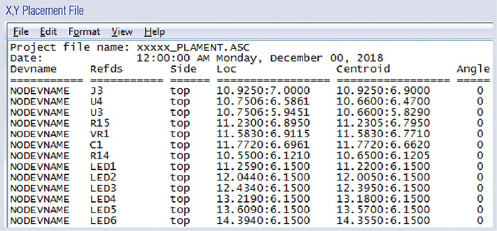
Figure 1. X,y placement file.
Solder paste stencil artwork file. Before any SMT parts can be placed on the board, the PCB must run through a printing process that deposits a thin layer of solder paste on the component lands. A solder paste stencil artwork file (FIGURE 2) is usually output in Gerber format from the source design layout and includes all the openings from which solder is screened onto the SMT pads.
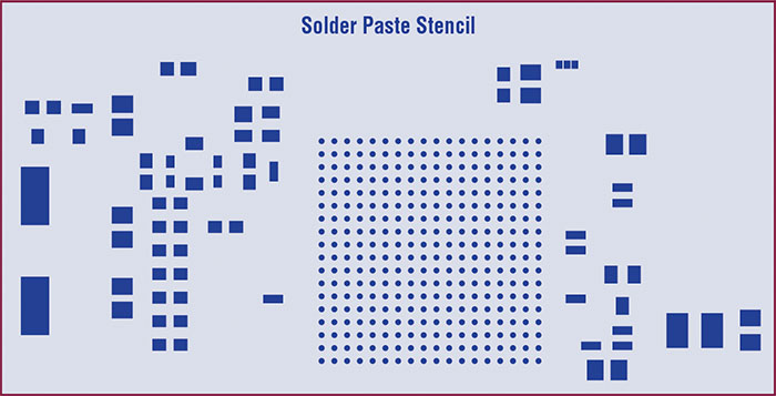
Figure 2. Solder paste stencil file.
Test point location file. If testability will be implemented on the PCBA, include a file that defines all test point locations for the test fixture supplier to build the equipment. Like the placement file, the test point output file can be very simple ASCII text. The file is output from the source design layout and derives its data from test point lands specifically identified for test. The file needs to include net names, side of access x,y locations, and test point names if applicable (FIGURE 3).
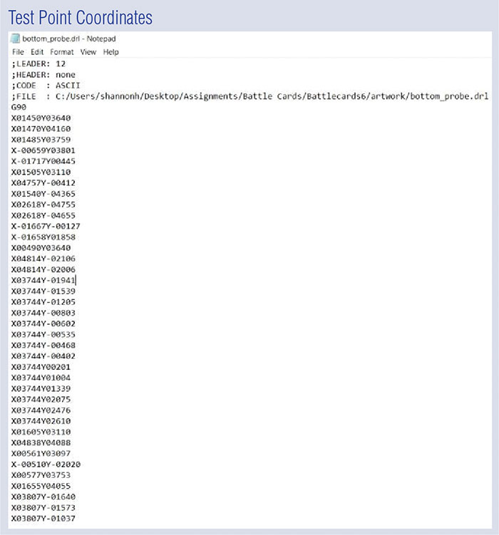
Figure 3. Test point file.
PCBA documentation. PCB documentation is critical to manufacturing success. Although data and machinery run the PCBA manufacturing assembly process, complete, graphic PCBA documentation begins the process. Tangible documentation reflecting what the data will produce is critical for quotation and setup reference. A complete PCBA document gives manufacturing stakeholders the ability to view the finished PCBA and start the assembly process with the end in sight. Additionally, the same helps to finalize the PCBA manufacturing process by giving the inspection stakeholders views and notation with which to evaluate the finished product.
The three essential elements of PCBA documentation are the schematic, BoM and assembly drawing.
Schematic. Documentation for the schematic is most likely the simplest act of PCB documentation. Since the schematic served as the source design file driving the layout of the PCB, the schematic becomes a “document” by simply placing a proper format around it. How this is provided, whether through a source file, paper copy or PDF usually depends on company culture. There are typically no extra details added to the schematic at the time of formal documentation.
The bill of materials (BoM). The BoM documentation is an official, formatted document that may be embedded inside a complex, corporate data management system. Documentation for the BoM is always output from the source: the schematic document. The part line items are pulled into a paper or electronic environment, which allows signature approval and formal release for distribution to purchasing, manufacturing assembly, and inspection stakeholders.
Assembly drawing. Like the PCB fabrication drawing explained in last month’s column, the PCB assembly drawing serves less to indicate how a PCBA is to be manufactured and more to specify how the assembly shall perform.
The job of the PCB assembly drawing is to show all the parts that will be assembled on its two outer surfaces. It is used as a guide for placement programmers and inspection personnel to measure how well the parts are placed on the board, how well the solder joints are formed and how clean they must be at the end of the process. How will the final inspection stakeholder know what is intended and expected without a clear, pictorially rich document that specifies design intent?
To serve as a viable manufacturing reference, the complete assembly drawing needs to include at least three key items to satisfy the needs of the assembly manufacturing stakeholders:
- Assembly pictorial
- Assembly details
- Assembly notes.
Fabrication vs. Assembly Documentation
Compared to having to specify the thousands of holes, trace layers and processes involved with bare PCB documentation, the documentation for a PCB assembly appears simple. The ones who will be finishing and inspecting the PCBA are going to appreciate the time spent on the front-end. If you have successfully completed and ensured the accuracy of the schematic and bill of materials, the efforts will “pay it forward” as they are fed into the creation of clearly illustrated, detail-rich, and simply notated assembly documentation.
Manufacturing panel. The PCB on screen at the time of layout will need to be multiplied into an array form (or panel) for volume manufacturing. To reduce manufacturing time, the manufacturing engineer will work with the PCB supplier to order the PCBs in an array form (FIGURE 4). A manufacturing panel array will make it possible for many PCBs to be processed together on a single manufacturing panel that carries all the PCBs down the manufacturing line together. An array of PCBs organized on a panel in a 3" x 5"configuration could yield 15 completed PCBAs after a single pass through the assembly line, effectively reducing the manufacturing run time for the PCBA to 1/15 compared to a single board (FIGURE 5).
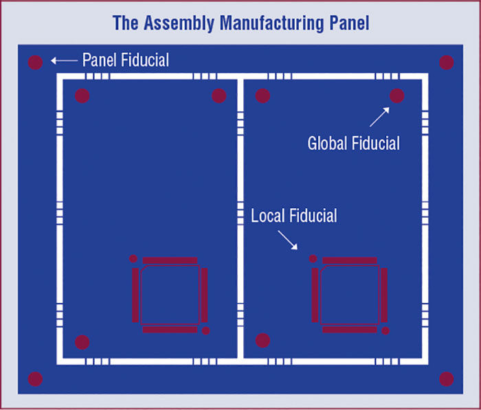
Figure 4. Manufacturing panel.
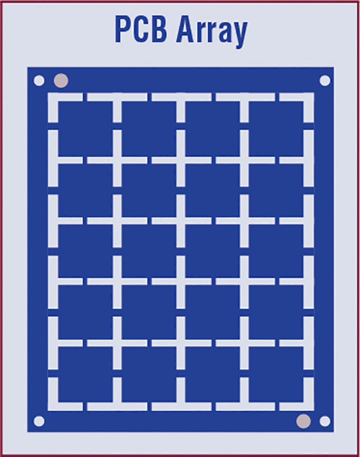
Figure 5. PCB array.
Besides a good overview of the PCB assembly process, what does a PCB designer need to do to create the best manufacturing panel array for the design? Surprisingly, very little. In fact, unless the design is going to be processed by the PCB designer’s own company, don’t do it.
Assembly paneling is best determined by the assembler, based upon its manufacturing requirements. If the designer does not know where the PCB is destined to be built and knows nothing about the provider’s equipment or capability, it is best to leave the design as a one-up and let the assembler do the rest to fit its process. The singulation method (sometimes referred to as excising or depaneling) of the finished PCBA must be determined based upon the board outline shape.
The process of singulation is accomplished using one of three common processes – v-scoring, tab-routing, or punching – each requiring unique panel design specifications.
If PCB designers have very little to do with the creation of the manufacturing panel array, why do they need to worry about it? Regardless of excising method used, the PCB assembler will need space inside the board edge to perform the operation. Therefore, it is important for the designer to understand the processes and requirements needed to create a manufacturable design. For example, often overlooked is the IPC recommendation to provide approximately 0.020" (0.51mm) clearance between the nominal PCB outline and all copper on the PCB to permit successful assembly.
IPC-2221 and IPC-2222 provides some excellent guidelines for helping they EMS provider create manufacturable, cost-effective panels from a design. For a basic understanding of the design process, following is an overview of common excising processes and what information to consider when designing.
V-scoring. V-scoring is accomplished by machining shallow, linear cuts on both sides of PCB panel, each defining the edge of the rectangular PCB. The depth of the cuts penetrates approximately 1/3 into the PCB from each side, leaving approximately 1/3 of the PCB material left to constrain the PCB in the panel during the assembly operations (FIGURE 6). After assembly, the panel is moved to a “pizza cutter” type device which utilizes a sharp, round blade to cut the remaining web material in the v-score and break the PCB free.
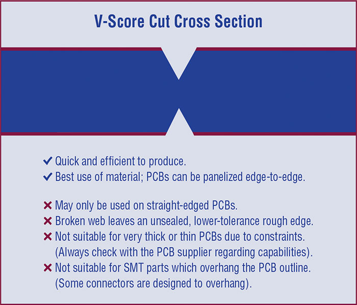
Figure 6. V-score cut cross-section.
Tab routing. For PCB designs that cannot tolerate v-score, tab-routing is an excellent option for the assembler (FIGURE 7). Tab-routing requires a certain amount of space around the PCB outline to permit a routing operation to remove all the material between the board edge and panel. Without a web, the individual PCBs would simply drop out of the panel, were it not for a few keenly placed “tabs.” The panel designer strategically places them around the PCB perimeter to “tack” and constrain the PCB within the panel. The tabs are formed by the high-speed routing tool exiting the route path for a few millimeters and then plunging back in to continue cutting the outline. Like the v-score webs, the tab-routed tabs remain in place throughout assembly. In the case of tab routing, the PCBAs are singulated using a pneumatic hook cutting-device, specially designed for removing tabs. The hook cutter enters from the bottom side of the PCB route and pulls downward on the tab, crushing the material away from the board edge.
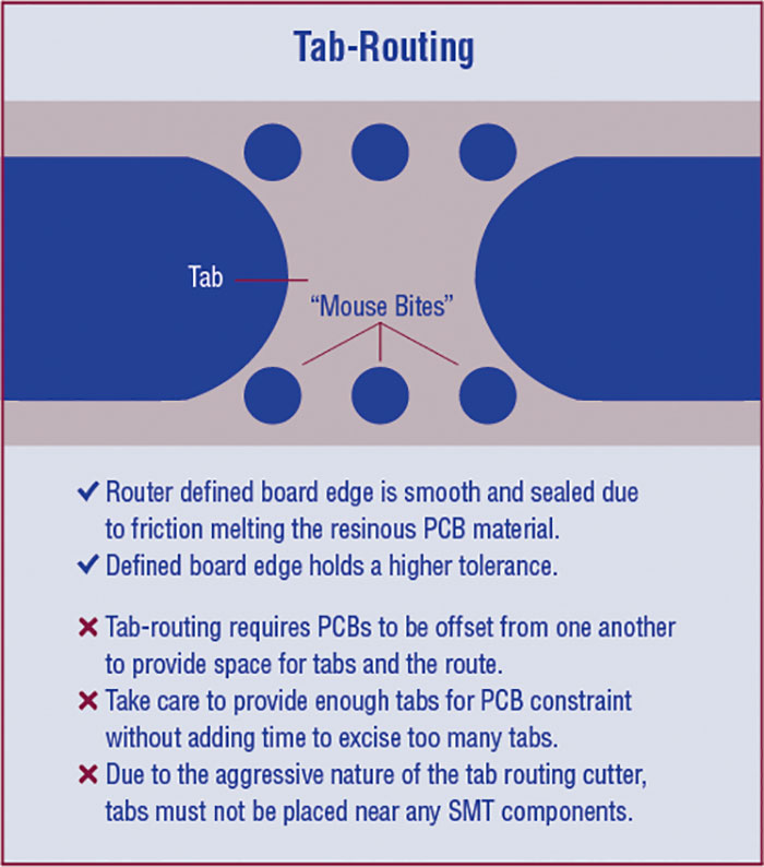
Figure 7. Tab routing.
Punching. On very high-volume PCBAs, a punching method can be utilized to shear the assemblies from the panel. This process typically requires the use of non-glass and non-fibrous material, such as the CEM family of laminates. There are very exacting design criteria which must be considered to provide allowances for the punch/die equipment to perform properly. It is highly recommended to contact the PCB supplier if there is any possibility for the punch excising method to be used.
If there is anything to learn from the disciplines of the manufacturing and assembly floors it is that a process of checks and verification must be in place at every step. While the designer does not have much involvement in the creation of the PCB array, to make sound design decisions it is important to understand what is involved. This way, when the design is ready for production, manufacturing hiccups can be avoided. Part two of this article will dive deeper into each step of the assembly process.
This excerpt of The Hitchhiker’s Guide to PCB Design was written by EMA Design Automation with of RocketEMS. Download to learn more about PCB design stakeholders and real-world, actionable PCB design tips from industry experts (go.ema-eda.com/pcbguide).


