QFN? QFP? QFWhat?

The names are similar but the layouts are not.
The QFN (quad flat pack, no leads) has become my favorite integrated circuit package. It’s very compact, yet is easier to use than a µBGA.
µBGAs of 0.5mm and smaller pitch become a bit more difficult and costly with more than two rows of pins. At those geometries, escape routing can involve plugged and plated vias, which add complexity and cost to the fabricated board. QFNs can be almost as small, but have all of the pins exposed around the edges, so there’s no need for escape routing.
One thing that’s important to note is that despite sharing the first two letters (Q and F), QFP and QFN footprints are not interchangeable. We do, from time to time, see boards laid out for one along with the other form packaged part.
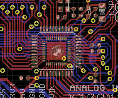
Take a look at this PCB layout clip from the Arduino Leonardo printed circuit board (FIGURE 1). It has both footprints on the board. You can see how much bigger the QFP package is.

Figure 1. This layout demonstrates the difference in land pattern size between the larger QFP and smaller QFN.
The Arduino designers put down both footprints because the Atmega32U4 chip used in the Leonardo sometimes has supply issues in one package or the other. This gives them the flexibility to use either without making changes on the board.
You might consider this as an option if there’s space for a QFP and you are concerned about the availability of one package variant or the other. If you do, there are some very important things to check out:
- Make sure the pin-outs match. Some parts vary the pin-out a bit between packages or have extra pins on one or the other.
- Make sure the extra space won’t cause noise problems. Generally, bypass caps should be as close as possible to the supply pins. In the case of the Leonardo, the extra distance when using a QFN part isn’t a problem, but in some designs it might be.
- Make sure the board won’t be in an environment where unsoldered pads will be a problem. Some harsh environments could attack the unsoldered pads. If that’s the case, consider conformal coat.
is marketing manager at Screaming Circuits (screamingcircuits.com); This email address is being protected from spambots. You need JavaScript enabled to view it.. His Twitter handle is @pcbassembly.


