Ten Steps to 10GHz

Properly compensating for high-frequency losses in the routed channels.
Serial links approaching 10Gbps are becoming more and more common in many PCB designs. Although there are a number of concerns working with busses at such high data rates, serial interfaces are simpler than parallel interfaces like DDR3 and DDR4. Differential serial data transmission eliminates a number of concerns that plague parallel busses, like power draw and timing issues, and can be more straightforward to implement if a handful of simple rules are followed.
1. Start with the right impedance. Most serial links are designed to operate on 100Ω impedance differential pairs. Not only is it important to use the correct trace cross-section to get 100Ω differential impedance, but it should also be designed to keep loss at a reasonable level. Though it is tempting to use 4- or 5-mil traces to maximize routing density, loss is entirely too high with such narrow traces. Wider traces are, of course, less lossy, but in order to meet impedance requirements, those wider traces must be used with thicker dielectric materials. Thicker dielectrics mean more spacing is required for crosstalk isolation. So, there are a number of design tradeoffs to consider when defining the trace cross-section, and using data from simulation can help ensure the right trade-offs are made. Some serial links, like PCI-Express, can be designed to run at a lower differential impedance, specifically 85Ω. This can aid greatly by permitting wider, less lossy traces, while still using thinner dielectrics.
2. Sweat the small stuff. Short discontinuities that can be ignored at slower speeds need to be taken into account for 10Gbps speeds. With edge rates on the order of 50ps – that’s about 300 mils long on a PCB – discontinuities fewer than 100 mils long can have a significant impact on the signal. The most common discontinuities are vias. After taking care to design traces and reference planes with the correct geometries to maintain a nice, uniform impedance, it is a little odd to send the signal through the board on a drilled, plated hole, but sometimes using vias is simply necessary for routability. Vias can be made closer to trace impedances by using smaller drill holes, removing nonfunctional pads, and spacing them apart appropriately. Routing traces at 85Ω helps, as the result will be much closer to a practical via impedance.
3. Avoid stubs. Stubs will kill a 10Gbps signal. That is why all high-speed serial interfaces are point-to-point differential pairs. Branching off for test points or debug connectors will add stubs, which excessively degrade the signal. Large pads can have a similar effect. And, again, vias must be designed appropriately. Vias are the most common place a stub might exist on a serial link. Via stubs can be greatly reduced by backdrilling – a method by which the metallized stub on the via is drilled out, toward the end of the manufacturing process. However, this involves some tolerance and will still leave a short stub on the via. To reach speeds of 10Gbps, it may be necessary to use microvias and/or blind/buried vias that leave no stub. Using this HDI (high density interconnect) technology adds significant cost to the design, of course, but results in a much cleaner design for both signal integrity and power integrity (Figure 1).
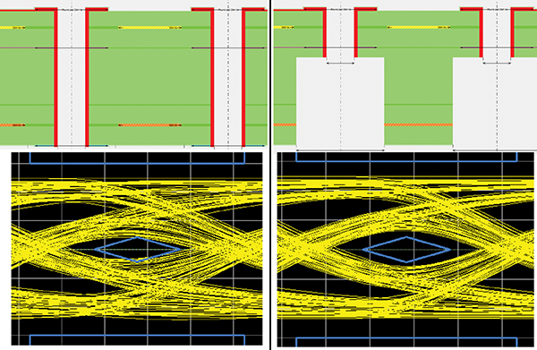
Figure 1. Eye diagrams of 10Gbps signal with vias with long stubs (left) and with backdrilled stubs (right).
4. Match lengths, tightly. To reap all the benefits of differential signaling, closely match the lengths of each trace in the differential pair. A matching constraint of 5 mils between + and - is reasonable; even matching to 1 mil is justifiable. If given the opportunity to get rid of a known source of skew, it should be taken. This may mean adding length to one side of the differential pair and “breaking” the differential cross-section momentarily, but as long as those compensation lengths can be kept very short, the overall resulting matching is worth it.
5. Match phase. In addition to total lengths, it is best to keep differential signals tightly “in phase” with one another. That means the signal edges are traveling next to one another. Stated another way, the length difference at any given point on the line should stay below a certain threshold. This is especially important when switching layers through a via pair. It keeps the differential pair from radiating and maximizes its noise immunity. Many layout tools support “in-phase” routing to ensure this is done correctly.
6. Space things out. Many serial interfaces consist of multiple pairs all traveling in the same direction, which can lead to dense routing. Use simulation to determine what spacing is needed for appropriate crosstalk isolation. Also, take advantage of the fact that the differential pairs are unidirectional, and interleave transmit and receive pairs so that forward crosstalk becomes inconsequential.
7. Isolate the differential signals. Single-ended signals can pose even more of a crosstalk threat than other differential signals. Even if they are operating in the MHz realm, these signals can still have fast edge rates. A 3.3V signal looks massive next to a differential signal operating in the hundreds of millivolts, so even a small amount of crosstalk from such a signal can cause big problems for the differential pair.
8. Use wide traces. As frequencies exceed several hundred MHz, there is a noticeable increase in trace resistance from skin effect resistance. This is because current will only occupy the outer periphery or “skin” of a trace at higher frequencies, effectively reducing the cross-section of the trace and increasing its resistance. This phenomenon is further exacerbated for GHz-range frequencies, where the surface roughness of the trace comes into play, and current is limited to occupying only the “peaks” on the surface of the trace. Using wider traces permits more “skin” to be occupied by the current (Figure 2).
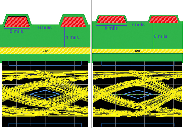
Figure 2. Eye diagrams of 10Gbps signal through 10” of FR-4 on 100Ω differential pairs using 5-mil traces (left) and 9-mil traces (right).
9. Keep it short. Shortest routes are best, as they reduce the amount of loss the signals will experience. Shorter routes also mean less exposure to crosstalk and outside noise that might affect the signal. The longer the routed length, the more important it is to minimize loss, and the possibility that more expensive dielectrics with low-loss tangents will need to be used in the design.
10. Emphasize and equalize. To achieve 10Gbps data rates, busses will employ signal conditioning techniques such as pre-emphasis or de-emphasis at the driver and some manner of equalization (like DFE or CTLE) at the receiver. These methods compensate for high-frequency losses in the routed channel. It is important to use the right settings for each individual diff pair in the design, and this is another area where simulation is an indispensable tool for predicting the right settings.
High-speed serial interfaces are much more straightforward to implement than parallel busses, as they have a much more finite set of problems. And though those problems scale as speeds approach 10Gbps, following these same 10 steps will permit successful implementation of serial interfaces at any speed.
is product manager for high-speed PCB analysis tools at Mentor Graphics (mentor.com); This email address is being protected from spambots. You need JavaScript enabled to view it..


