Effectively Managing PCB Design Constraints

Constrain what is necessary, but don’t go overboard.
Back in the printed circuit board’s early days, before EDA tools were even necessary, constraints were handled verbally. The engineer would carry the schematic to the PCB designer and concisely state the constraints: “Can you fit this on a 4x6" board?” That’s certainly not the best way to communicate constraints, although I would guess there are instances when the design still needs little more communication than that.
For the most part, specifying a set of constraints has come with several important benefits. First, design quality will be improved since those important parameters will be met. Second, specifying important constraints usually means the design will be completed more quickly. And finally, the improvement in quality also means there is less likelihood of having to respin the design due to signal integrity, power integrity, or EMC issues. There is one important downside: Over-constraining a board can make placement and layout more difficult, complicating autorouting, and potentially adding time and even layers to the design. So, it’s important to constrain that which is necessary, but not go overboard.
Beyond the simple constraint of PCB dimensions, sophisticated constraint rules are now frequently specified for routing and clearances, trace length, vias, individual nets, groups of nets, and even groups of pins. Constraints can be nested and even entered with conditional parameters to allow them to be evaluated within the context of the design.
Most PCB designs do have constraints, and some very high-speed designs may be highly constrained. As constraints grow in number, more sophisticated tools accelerate the task on constraint entry and management.
Setting constraints. Constraint management tools range from the simple to the robust. As one would expect, the more robust tools generally have features that make them easier to use and are more tightly integrated into the entire design flow.
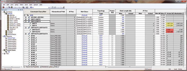
Virtually all tools have a “spreadsheet mode” (Figure 1). Using this method, the engineer and designer define components that must be constrained. Then, signal names are entered into the spreadsheet format, along with the values or rules to be followed. In this spreadsheet, first constraints for differential pairs are entered, in this case maximum and minimum lengths. Next, reused circuitry is listed and the constraints for connecting the reuse circuit are specified; constraints assigned to the circuit being reused are embedded within that circuit’s design.

Figure 1. The spreadsheet mode is very popular for entering constraints.
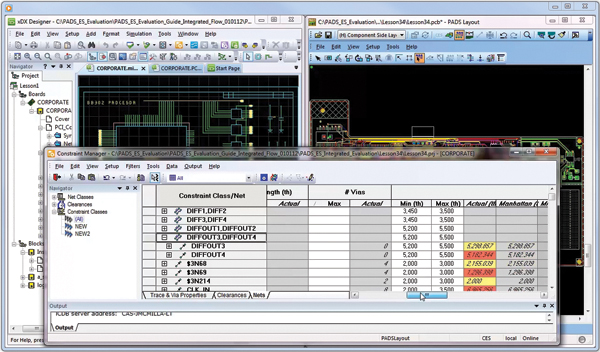
Most PCB designers are probably already familiar with entering constraints in this manner. Newer tools present a user interface with much easier to use formats, permitting even projects with a large number of constraints to be quickly entered. Figure 2 illustrates the more robust, contextual way of entering constraints. Here, the designer has imported the schematic and has begun placing parts. By simply clicking on the area of the schematic where constraints are to be specified brings up the constraint manager. Constraints can easily be entered, and then the designer can return to the layout process with the constraints being enforced.

Figure 2. More sophisticated tools offer interactive constraint management right from the schematic. They also support simulation, permitting constraints to be examined and optimized.
The most sophisticated tools allow the designer to select a net or part of the circuit and then instantly open a simulation tool to examine the effects of constraints on that selection. Driver strengths can be adjusted, transmission lines modeled and simulated, and the effects can be analyzed. Constraints can be adjusted until the desired result is attained. Then, those constraint values can be entered into the constraint manager and used to drive the layout of the PCB.
Finally, tools entering today’s market are also much more intelligent than that of the simple spreadsheet. They have a great deal of intelligence behind an easy-to-use GUI, allowing a designer to produce valid, accurate results and use those results to specify constraints and lay out the board, without input from signal or power engineers.
John McMillan is Pads technical marketing engineer at Mentor Graphics; This email address is being protected from spambots. You need JavaScript enabled to view it..


