Improving Signal Integrity with Microvias

Blind, buried or smaller-sized holes can reduce plane voids and insertion loss.
High density interconnect technology can increase design density and reduce overall board size. It can also improve the signal and power integrity of a PCB. Here are two case studies that show how blind vias, buried vias and microvias can be used effectively.
Case 1: Improve power integrity by reducing voids in planes. High-power designs for high-speed digital signals require low impedance PCB power planes for proper operation. Therefore, solid planes for power and ground are always preferred. In many cases the power and ground planes under a BGA component have voids, as a result of through-hole vias. These voids have negative effects on power integrity, such as:
- Increased plane inductance.
- Increased plane resistance (as IR drop from power supplies to BGA pads).
- Decreased plane capacitance.
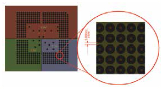
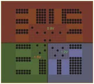
Figure 1 shows how 8mil through-hole vias under a 0.8mm-pitch BGA have created voids in the three split power planes. The copper webs between the voids are just 3.5 mils wide. By replacing the through-hole vias with blind or microvias, the plane voids can be reduced (Figure 2).

Figure 1. Voids and split power planes under BGA component.

Figure 2. Voids eliminated with HDI technology.
Case 2: Improve signal integrity by eliminating via stubs. At speeds of 5Gbps or 2.5GHz and faster, via stubs begin to have a noticeable impact on the insertion and return loss of a PCB. Through-hole via stubs can be removed mechanically in some applications, but in the case of PTH high-speed connectors, such as backplane connectors, pins cannot be back-drilled. One solution is to use surface-mount high-speed connectors and blind vias (Figure 3).

Figure 3. Through-hole via stub, before and after.
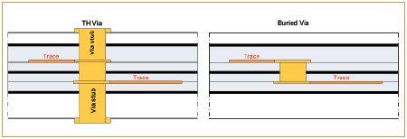
Figure 4 shows two via stubs in both ends of a through-hole via for layer exchange of striplines. Buried vias, then, can be employed to eliminate the stubs.

Figure 4. Through-hole via stub, before and after.
In these cases, the use of blind vias and buried vias completely eliminates the through-hole via stub, improving the signal integrity of the PCB.
These are just two situations where HDI technology enables a layout designer to produce better quality PCBs. With recent advancements in PCB manufacturing capabilities, look for many more case studies to come.
Pi Zhang is a senior design engineer at Nuvation Engineering (nuvation.com), a design firm specializing in electronic design services and product development; This email address is being protected from spambots. You need JavaScript enabled to view it..


