Ever Use a TI X2SON Packaged Part?
 As chips get smaller, the package designers are getting creative in their effort to make room for component leads. Texas Instruments’ new X2SON package sports triangular footpads in a pattern that I’m not sure I’ve seen before. X2SON stands for extra small outline no-lead. In my experience, TI is one of the better companies insofar as testing and documenting manufacturability is concerned. The datasheet for this device (ti.com/lit/an/scea055/scea055.pdf) is no exception.
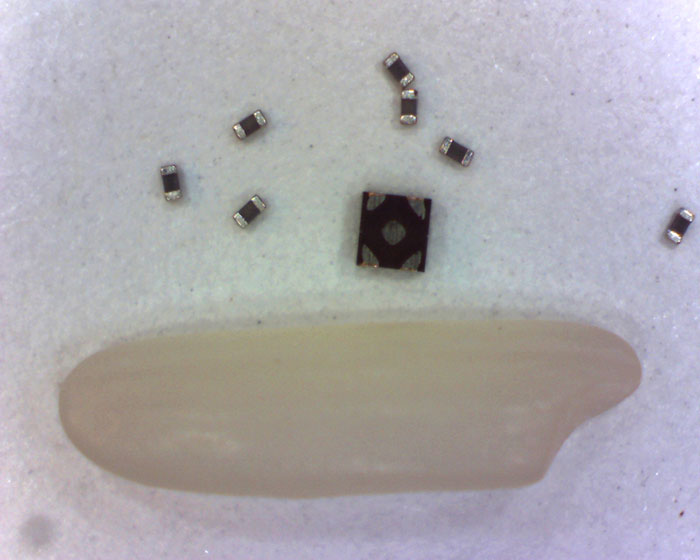
FIGURE 1 shows the five-leaded TI part in contrast to a grain of Jasmine rice and a few 01005 ceramic capacitors. (I’m selling the capacitors for $500 each. Just kidding.)

Figure 1. A TI X2SON, shown adjacent to 01005 capacitors and a grain of Jasmine rice.
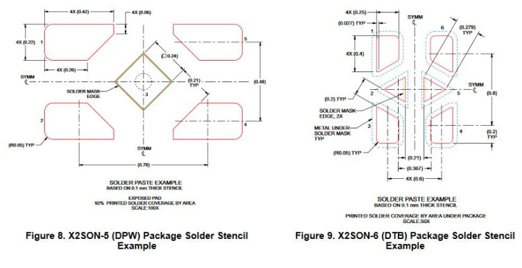
The part is 0.8 x 0.8mm with the five leads. TI suggests either a 4 mil (0.102mm) trace coming out of the center pad or a 4 mil via in the pad to escape the center pad. (The via must be filled and plated at the fabricator.) TI also does a nice job detailing the solder paste stencil layer, as in FIGURE 2.

Figure 2. Solder stencil example for the extra small outline no-lead device.
Designers will most likely need a custom CAD footprint for one of these. Either very carefully do it yourself or go to a known good source for land
patterns. If such a source doesn’t already have it in its library, it will make it for you.
These small packages aren’t going away. We’re only going to see more of them. They may seem intimidating, but with a good footprint and a competent manufacturer they aren’t so bad.
is marketing manager and chief technology champion at Screaming Circuits (screamingcircuits.com); This email address is being protected from spambots. You need JavaScript enabled to view it..


