Where to Put Panel Tabs

First rule of panel tabs: keep them away from connectors.
Many small quantity PCBs are ordered individually cut. They come to the assembler as a set of unconnected boards. For small quantities of reasonable size boards, it makes the most sense to order them this way. However, for really small boards, and larger quantities (for example, 50 or more), purchasing boards in a panel (also called an array) is more appropriate. It reduces errors and assembly time.
There are a few additional factors to consider with panelized boards:
- First, don’t create a panel in the CAD software. Instead, lay it out as a single board and have the fabricator put it in a panel. This ensures the most efficient use of PCB space, and the fabricator will create the files in the format the assembler needs.
- Avoid family panels. A family panel is when several different board designs are put on the same panel. The boards in family panels often repeat reference designators, which causes problems at assembly.
- If there are overhanging parts, such as the increasingly common micro USB connector, make sure the panel tabs aren’t placed near them.
Some components, such as certain connectors, have protrusions that will keep them from lying flat on a panel tab. In all cases, even without the protrusions, the operation of separating the panels with a component on the tab can weaken the component solder joints, or even pop them off the board completely.
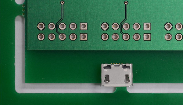
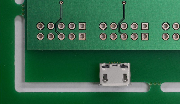
FIGURE 1 shows how not to do it. Instead, make sure the tabs don’t end up under an overhanging component. Move the tab, as in FIGURE 2.

Figure 1. Panel tabs under a component, as shown here, can weaken the solder joint.

Figure 2. The better design is to put them away from the overhanging component.
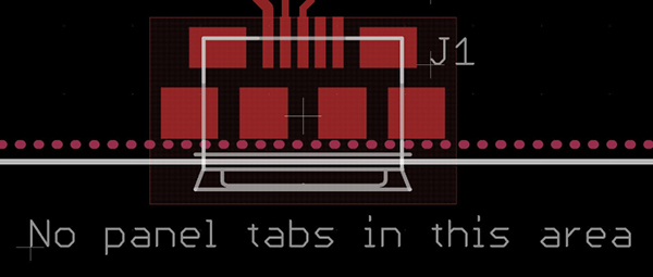
I asked our partner company, Sunstone Circuits, how to control where the tabs will be placed. They suggested putting this instruction in the document layer of the CAD file, or in a separate document covering fabrication instructions. In the CAD image (FIGURE 3), the overhanging component has a keepout area. The document layer has instructions to keep panel tabs out of the area.

Figure 3. A note in the CAD file can alert the fabricator to the keepout area.
is marketing manager at Screaming Circuits (screamingcircuits.com); This email address is being protected from spambots. You need JavaScript enabled to view it..


