Can the Right Alloy Prevent Tin Whisker Formation?


Phase 2 of our study involved wetting balance, spread, DSC and mechanical tests.
We’re continuing our summary of a year-long experiment aimed at identifying lead-free solder alloys that mitigate tin whisker growth. This study cut right to the chase, beginning with an elimination round. The first phase knocked out two-thirds of the nine original candidate alloys based on their whisker production.
The results of the tests were both intriguing and enlightening, and forced us to rethink what we thought we knew about tin whisker propagation. The investigation focused on the conventional wisdom that tin whiskers are the result of compressive stresses caused by electroplating, bending, intermetallic growth, and thermal expansion mismatches.
It assessed the influence of these most commonly cited potential causes by creating test specimens with wire dipped in molten alloy and bent after cooling (Figure 1), and then subjecting them to thermal cycling and environmental storage conditions.
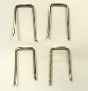
Figure 1. Tin whisker test specimens.
The dipped specimens grew whiskers, thereby eliminating the residual stresses of electroplating as the sole cause. Whiskers grew all over the test specimens’ bent area, including the outside – or tension side (this is still under debate) – of the bend, challenging the notion that they are a form of relief from compressive stresses.
Whiskers are becoming better understood to grow in locations where the grains of the tin are less mobile. When tin confronts a non-moving section, it tends to squeeze out at that location. This mechanism can occur many levels away from the source of the original driving force.
Thermal excursions did not produce whiskers, either. What caused the most whisker growth? High heat and humidity storage conditions. The effect of the environmental storage on whisker growth was unmistakable. All the lead-free solders grew whiskers under the most adverse storage conditions, but some grew more than others. More details on that first phase of the study can be found in our May column (circuitsassembly.com/cms/component/content/article/159-current-issue-articles/15973-tech-tips).
The next phase of the study tested seven alloys. It took the top three performers from Phase 1, added a few tweaks to those compositions, and the SAC 305 control, and put them through a variety of tests, including wetting, spread, differential scanning calorimetry (DSC) and mechanical properties.
Wetting balance tests offer both numerical and visual results. Numerically, they demonstrate the alloys’ different wetting forces, the faster wetting at higher temperatures of most alloys, and the slowing effect that aluminum has on wetting speeds (Figure 2). Visually, they show the alloy’s propensity to oxidize in air environments by their appearance on the wetting test coupons: Smoother appearances indicate less oxidation (Figure 3a), whereas the more textured surfaces indicate more oxidation (Figure 3b). “Tails” coming from the coupon (Figure 3b) are also a sign of oxidation and can indicate sluggish drainage properties.
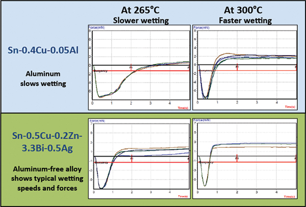
Figure 2. Wetting balance curves show wetting speed and force.
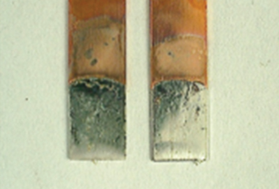
Figure 3a. Wetting balance test coupon shows smooth, unoxidized solder surface and minimal tailing. Alloy is Sn0.6Ag0.7Cu3Bi.
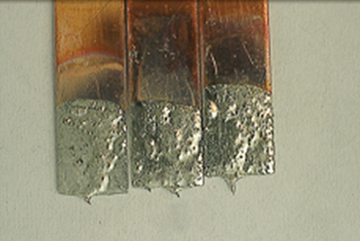
Figure 3b. Wetting balance test coupon shows rough, oxidized surface and “tailing.” Alloy is Sn0.5Cu0.2Zn3.3Bi0.5Ag.
Small-scale laboratory wetting balance tests can provide a lot of insight on production soldering performance:
- In wave and hand soldering, higher wetting forces signify better hole fill properties, and tailing implies a susceptibility to bridging and icicling.
- In reflow soldering, the sensitivity of wetting speed to melt temperature helps define the relationship between peak temperature and time above liquidus to optimize thermal profiles.
- In any type of soldering, oxidation rates indicate the solder’s compatibility with air environments. Alloys that oxidize rapidly may need nitrogen environments in wave soldering. They may or may not need nitrogen in reflow soldering, because the reflow process is more forgiving due to its long-acting fluxes and lesser opportunity for oxidation.
The IPC spread tests on copper all showed acceptable performance with no solder balling. The coupons were later used for thermal aging tests in Phase 3.
DSC testing identified the melting points, pasty ranges and undercooling properties of the alloys. The seven alloys tested had melting points between 201° and 227°C and pasty ranges between 11° and 21°C, making them all viable candidates for electronic soldering operations. Note that SAC 305, the most common lead-free electronic solder, exhibited a melting point of 227°C and a pasty range of 13°C when measured with the same techniques.
Hardness, tensile strength and elongation were measured and reported as part of the test protocols; however, there are no clearly defined specification ranges for the mechanical properties of electronic solders. These characteristics have little influence on the mechanical performance of components with leads, and only minor influence on leadless devices. In general, harder or stiffer components, such as those with ceramic bodies, need softer solder alloys to mitigate pad cratering, and softer substrates, such as flexible PCBs, typically benefit from more rigid solders that do not flex as easily.
The study’s third phase investigated intermetallic compound (IMC) growth kinetics. It aged the spread test coupons at 150°C for 24, 96, 288 and 740 hr., cross-sectioned the samples and measured the IMC thickness using optical microscopy. The results indicate that:
There is no correlation between IMC growth rates and whisker formation. SAC 305 demonstrated the worst whisker production but only average IMC growth rate.
All IMC growth rates were within a predictable range. They varied linearly with the square root of time (t0.5), and all alloys tested fell within the max and min curves shown in Figure 4.
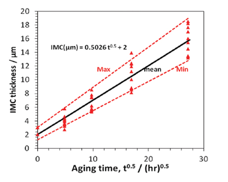
Figure 4. IMC growth kinetics at 150°C.
We generated, collected and analyzed a lot of data. What did we find? We’ll summarize the complete results in our upcoming conclusion to this series, but it all boils down to using the right alloy composition. Everything we’ve seen so far indicates that tin whiskers can be almost completely eliminated when the right elements are added to the tin.
Karl Seelig is vice president of technology at AIM Solder; This email address is being protected from spambots. You need JavaScript enabled to view it.. Tim O’Neill is regional manager at AIM.


