A Lean NPI Journey
How a designer/assembler migrated from conventional layout to a more efficient, concurrent DfM process.
Optimum Design Associates designs printed circuit boards following a standardized design flow to ensure customer requirements are met, quality levels are high, and the designs suitable for fabrication, assembly and test.
Optimum is implementing Lean NPI, which we believe is the only way to survive in the competitive field of PCB design and manufacturing. While the process is not yet fully implemented, we describe our journey and near-term plans as a template for what we believe will be the standard procedure for electronics product design.
Optimum’s vision is to offer customers a service following the “Lean New Product Introduction (NPI)” product development model. Lean NPI combines concurrent DfM analysis using vendor-supplied rule sets during the PCB layout process and the adoption of intelligent data transfer as the manufacturing output for hand-off to fabrication and assembly.
The Lean NPI process will provide a number of benefits to Optimum, including reduced time-to-manufacture, increased quality, and easier management of data packaging and handling.
We have already begun the Lean NPI journey by employing concurrent DfM during the PCB layout flow. Running DfM at key stages in the design saves time and effort during NPI. In the final step of Lean NPI adoption, working closely with manufacturing vendors and running DfM based on their rules will show improvements in quality and yield.
Let’s look at Optimum’s PCB design flow and transfer to manufacturing before a more detailed look at Lean NPI and its implementation.
PCB design process. Although Optimum has several PCB design tools available, depending on customer compatibility and fabricator requirements, Mentor Graphics tools have been the mainstay since the business was founded in 1991. Currently, we employ Expedition Enterprise and PADS.
The PCB layout process flow used at Optimum is shown in Figure 1. When PCB layout begins, the first step is to validate the bill of materials (BoM) using Mentor Graphics Valor NPI and Valor Parts Library to check that all part numbers, reference designators and quantities are correct and that package models are available for later use in the design flow. Missing package models can be generated at this early stage. Once component placement is completed, the design is subject to DfM verification using the same tools.
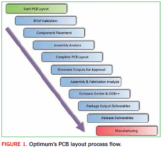
On completion of layout, provisional outputs are generated and delivered to the customer for design approval. In parallel, a comprehensive fabrication and assembly DfM analysis is performed. The results are used to confirm that there will be no quality or process issues during fabrication and assembly of the product and to ensure maximum possible yield.
Some companies do not use DfM analysis until the design reaches the fabricator, primarily to ensure acceptable yields of bare boards. If significant problems are found, the project must go back to design for a re-layout and then back to the fabricator. This can take days or weeks and incur a hefty cost.
Optimum has embraced the concept of concurrent DfM within the PCB layout process flow. By moving the DfM as early in the product design as possible – running partial checks on available data – problems are relatively easy to correct, and cost very little in either time or money compared to having a complete re-spin. At key stages of the design, the layout is examined at multiple points to assess the viability of both fabrication and assembly, which ensures the design meets the capabilities and process constraints of the manufacturer.
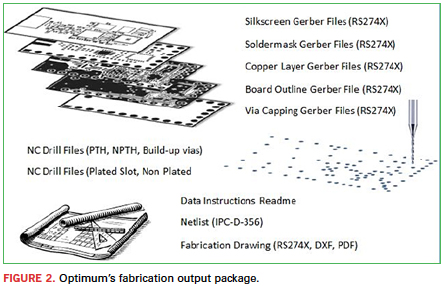
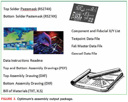
The last step in the PCB design phase is compiling the electronic files to deliver to the fabricator. Optimum produces an ODB++ output file as well as Gerber-based file sets. To ensure consistency between the DfM-verified ODB++ data and the traditional Gerber and Excellon drill outputs, Optimum conducts a graphical comparison. Once verified that both output formats are graphically identical, the final deliverable data are packaged and released to the customer and the fabricator. In addition to producing data packages for fabrication (Figure 2), Optimum produces assembly (Figure 3) data packages.
The aforementioned might be called the “standard” NPI process; that is, what most leading designers and fabricators are implementing today. As we described, Lean NPI is the next segment in the journey to become a complete Lean NPI-driven design and manufacturing entity. There are various levels of DfM that can be executed during the NPI process:
Level 0 DfM is performed on the factory floor where the product build is attempted and DfM problems are discovered. This method of verification is time-consuming and expensive.
Level 1 DfM is performed by the manufacturer using software tools and is a reasonable method to ensure the design complies with manufacturing rules and process constraints. The downside to this level is that the design organization is completely reliant on DfM feedback from the manufacturer. This feedback is used to make necessary design changes but may not include details about the design that could affect product yield or reliability.
Level 2 DfM is the ideal scenario, where DfM is executed during the design process using manufacturer-derived rules and process constraints. Not only can critical DfM errors be addressed during design, but improvements can be made to increase yield and reliability before committing to production runs.
The most efficient method of implementing DfM is to adopt concurrent DfM engineering. The PCB layout is designed in stages: placement, critical routing, final routing/planes. At each of these key stages: DfM analysis is executed. It can be very difficult and time-consuming to correct DfM problems after the layout is complete.1
Best practice Lean NPI process model. Lean NPI is defined by three enhancement elements within the “Best Practice Standard NPI Process Model.” First, ODB++ data are used as the preferred format for manufacturing hand-off because it contains product model intelligence, thus enabling high levels of automation. The second element is to execute concurrent DfM at key stages during PCB design development. The final element for Lean NPI is to execute DfM at Level 2. Figure 4 shows Optimum’s model, which is the template to which we are working.
[Ed.: To enlarge the figure, right-click on it, then click View Image, then left-click on the figure.]
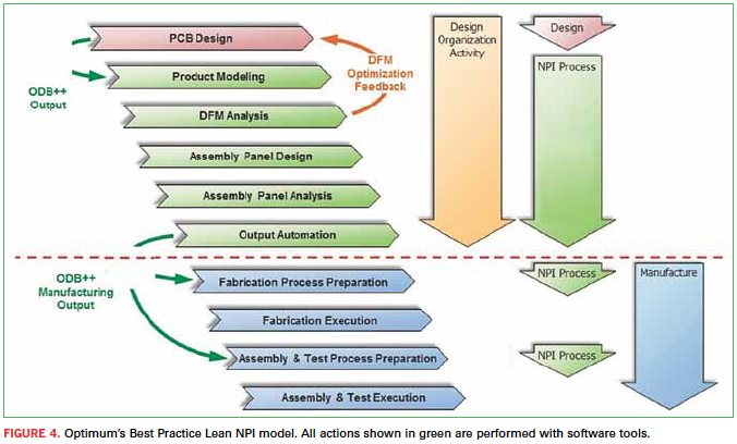
The layout is designed in stages and concurrent Level 2 DfM analysis is executed. When the layout is complete and any DfM problems resolved, the assembly panel is designed and validated. The final manufacturing output is generated and released for manufacturing process preparation.
Lean NPI process flow. During the collaboration with Mentor, some areas of Optimum’s business process have been identified where improvements can be made to achieve Lean NPI. By merging our PCB layout process flow with the Lean NPI process model, we derived the Lean NPI Process Flow (Figure 5). Although it may appear complex at first, many of the steps in the flow are fully automated.
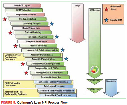
At the beginning of the design, the BoM is validated. This ensures all packages are available. If new packages are required, these can be generated while the component placement is performed. The completed placement is then subject to initial assembly analysis.
If DfM problems exist, they can be fixed before continuing with any complex routing. Prior to each analysis stage, product modeling adds attributes to the
manufacturing data, which enables comprehensive DfM checks to be executed, and also defines exactly what is to be manufactured such as layer stackup, copper weights, solder mask color and component assembly instructions. This removes the need for many drawings and documents traditionally used to communicate deliverables to the manufacturer. All product modeling activities are automated and repeatable.
Any critical routing can then be added to the design. On completion of the critical routing, an initial fabrication analysis is run. This highlights any DfM problems associated with the critical nets that need correcting before continuing with general routing. Clearly, critical routing should not be disturbed at a later stage due to DfM problems, as it may be very difficult to make changes while retaining signal integrity.
Next, the remainder of the routing, copper areas, power and ground planes and silkscreen legend (if applicable) can be completed. A final DfM analysis is run for fabrication, assembly and test that captures any DfM problems with the completed layout.
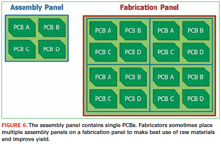
Once all DfM problems are investigated and corrected on the single PCB design, the assembly panel design and panel DfM analysis can be performed. This is an optional step offered by Optimum. Figure 6 illustrates the difference between the assembly panel and fabrication panel. The assembly panel is the fabricator’s deliverable and is used by the PCB assemblers. The assembly panel usually contains an array of single circuit boards. The fabrication panel contains an array of assembly panels and is only used to suit the fabrication processes and make best use of their raw materials.
Finally, the complete data package goes to the customer for final approval. During the approval process, if the customer requires Gerber data, we compare the Gerber output against the master ODB++ output to ensure that the data are graphically identical. Thus, the traditional Gerber data can still be used as a valid if less-efficient alternative in manufacturing process preparation. On receipt of customer design approval, the final manufacturing data are packaged and delivered to the manufacturer.
Remaining steps. During study of the PCB layout process flow, areas were identified where changes could be made to fully implement the Lean NPI process model. Key areas where Optimum’s business process could be modified are:
Optimum’s PCB design and NPI process would be enhanced by adding a DfM analysis stage when the critical routing is complete. This would ensure no DfM problems exist with the critical nets. If DfM problems do exist, they could be corrected and signal integrity retained. If DfM problems are discovered with the critical nets at a later stage it may be difficult and time-consuming to fix the problems without disturbing other routing or even component placement while retaining signal integrity.
The customer-approval stage could be moved to after the final fabrication and assembly DfM analysis step. This will ensure that the output data used for customer review and approval not only meet the electronic design specifications but are also fully manufacturing-compliant. Otherwise, changes may need to be made during the final DfM validation stage that the customer may not be aware of. This change to the process flow will also enable the customer to check and approve the manufacturing data – exactly what is to be manufactured.
Ensure exclusive use of ODB++ output data format throughout the flow from design to manufacturing process preparation. This would enable a more efficient data hand-off to both Optimum’s external fabrication partners and internal assembly and test lines.
As with any significant changes in design methods or business processes, there need to be metrics in place to measure performance improvements and show the effect of those changes on the performance of the business. We are currently developing and will be compiling performance and quality metrics that will be analyzed and discussed in a future article.
References
1. Matt Kelly and Mark Hoffmeyer, “Lead-Free Assembly Design for Manufacturability Considerations,” PCD&F/CIRCUITS ASSEMBLY, February 2013.
Randy Holt is a senior PCB designer at Optimum Design Associates and a former “Top Gun” winner at PCB West; This email address is being protected from spambots. You need JavaScript enabled to view it..


