Addressing ‘Power-Aware’ Challenges of Memory Interface Designs
The combination of complete model libraries, advanced tools and engineering expertise addresses modern buses and data rates.
Memory interfaces are challenging signal integrity engineers from the chip level to the package, to the board, and across multiple boards. As the latest DDR3 and DDR4 speeds support multi-gigabit parallel bus interfaces with voltage swings smaller than previous generation interfaces, there is no room for error in any modern memory interface design.
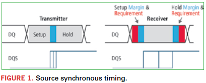
Designing a memory interface has always been about timing closure. Each data signal’s timing needs to be compared to its related strobe signal in such a way that the data can be captured on both the rising and falling edge of the strobe, hence the term double data rate (DDR). The increase in data rates to more than 2 Gbps has made the timing margin associated with each rising and falling edge much smaller (Figure 1).
However, today’s biggest challenge comes in accurately measuring timing while considering the fluctuations in power and ground rails that occur due to simultaneously switching signals. In the worst case, when all 64 bits of a data bus transition simultaneously, large instantaneous changes in current across the power distribution networks (PDNs) cause fluctuations in voltage levels that impact the timing margins of the transitioning signals. These signal switching variations are often called timing “push-out” or “pull-in.” If the time between data settling and the strobe transition is too much, meta-stable conditions can occur that would impact the data integrity (Figure 2).
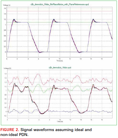
Characterization of simultaneous switching noise (SSN) effects requires system-level transient analysis, including transmit and receive buffers and all interconnect in between. Unlike for SPICE, real circuits may not apply a global ground (node 0) and all signals are referenced to local power/ground pads. Therefore, not just the interconnect, but the associated PDN must also be included in this system model.
The system interconnect includes an on-chip path from the active silicon transmit buffers to external die pads, the package, a PCB and possibly a motherboard; the same components are on the receive side of the system. The on-chip portion of the system is typically modeled as a spatially distributed, lumped RC (more recently RLCK) SPICE circuit. Low-speed packages are represented by RLCK lumped models and higher frequency packages by S-parameters. PCBs are large enough that lumped element models rarely apply, and S-parameters are typically used. These non-lumped, broadband frequency domain models imply a difficult transient simulation even without the nonlinear buffers included.
Because most signal integrity (SI) software tools were created in an era when the timing effects of SSN could be ignored, many tools perform SI analysis assuming ideal power and ground rails. However, with the margins becoming so tight, assuming ideal power and ground could cause prototypes to fail or, worse yet, data integrity problems on production hardware in the field.
The trend in SI engineering is to analyze memory interfaces considering the effects of signal and non-ideal power/ground. This is now being referred to as “power-aware” SI analysis. Modeling of I/O buffers can now follow an updated IBIS standard (IBIS 5.0+) where power-aware IBIS models permit SI tools to consider the parasitics of the power and ground connections as well as the signals.
Here, we discuss the I/O modeling, interconnect modeling, simulation, and analysis challenges associated with power-aware SI of today’s high-speed memory interfaces and how modern tools can be used to address these challenges.
Power-Aware I/O Modeling
Transmit and receive buffers are critical intellectual property to both fabs and fabless design companies. They are either extracted at a detailed netlist level by cell characterization software or carefully crafted manually by I/O designers. These models are then encrypted and distributed only under strict nondisclosure agreements. Each individual buffer includes many transistors. These buffer circuits suffer from slow convergence during SPICE simulation even with ideal lumped loads.
Full-bus SSN characterization requires hundreds, in some cases literally thousands, of transistors combined with broadband frequency domain models. Such simulations are extremely resource-intensive and sensitive to SPICE convergence issues. Typical simulation times are measured in days and memory consumption in double or even triple digit gigabytes when performed on high-performance computer platforms.
IBIS buffer macromodels are commonly applied for system-level SI simulations instead of transistor-level netlists. Simulation time, memory consumption, and convergence issues are all dramatically reduced versus transistor-level simulation. However, in the past it has been well known that IBIS models are not amenable to SSN simulations because 4.2 and previous versions did nothing to ensure proper power/ground buffer currents.
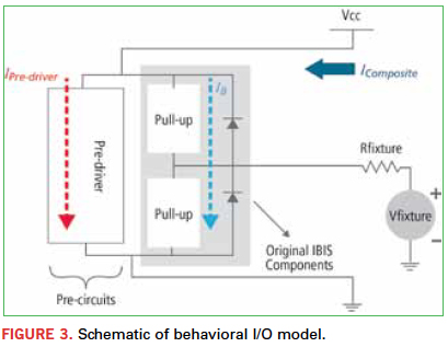
IBIS 5.0 was enhanced to address this situation. Updates called BIRD-95 and BIRD-98 were added to the specification to model power currents and their fluctuations with respect to PDN voltage noise. Together, these two updates provide an accurate modeling of buffer power currents and enable IBIS 5.0-compliant models to be applied for full-bus SSN characterization (Figure 3).
Not all SI software presently supports application of IBIS 5.0 buffer models for power-aware SI analysis, but it is becoming more common. Commercial solutions are now available to support conversion of transistor-level buffer models to IBIS 5.0 behavioral macromodels (Figure 4).
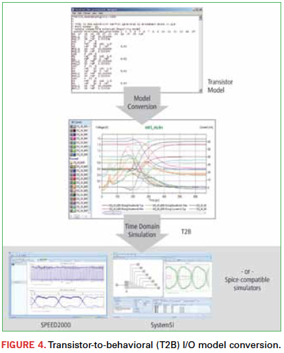
These are easily applied by fabs, fabless design companies with their own IP, and even designers who may be provided only transistor-level models. Semiconductor vendors are moving toward providing IBIS 5.0 models. If such models are not available from their website, they may well be available for internal application or distribution to designers under nondisclosure. IBIS 5.0 buffer models address IP sensitivity issues that exist for transistor-level netlists (even encrypted netlists) and eliminate the need to disclose process parameters.
Interconnect and PDN Modeling
One of the key challenges in enabling a power-aware SI methodology is extraction and modeling of the interconnect, for example PCBs. Historically, this has been done by extracting transmission line models (e.g., SPICE “W” elements) for signal traces, while assuming they are routed adjacent to an infinite, solid reference plane. Signal vias are often modeled using a fast closed-form approach as isolated, uncoupled objects with only self-parasitics (i.e. ideal return paths). This kind of technique is very convenient mathematically, as it enables extractions that are relatively inexpensive from a computational standpoint. However, this approach completely ignores the power delivery network (PDN), forcing an undesirable “ideal power” assumption upon the simulation and masking any PDN effects from the simulation results.
Incorporating the PDN into the extraction process is a significant challenge. This involves the extraction of the copper shapes that typically comprise the power and ground planes, as well as vias that run through them, along with the coupling to the signal traces. These vias essentially act as radial transmission lines that excite the parallel plate plane structures, perturb the power supplied to the chips, and couple noise back onto the signals as well.
Decoupling capacitors must also be modeled and incorporated into the extraction, as do models for the voltage regulator module (VRM), which is where power is brought into the PCB from the external world. Once the extraction problem expands from “signals and vias” to “signals, planes and vias,” the simple transmission line extraction techniques historically used are no longer applicable, and the problem requires some kind of full-wave-based solution.
Traditional full-wave field-solvers address the full set of Maxwell’s equations, with no (computationally) simplifying assumptions. Full-wave engines are certainly able to handle all the structures discussed previously, but come at a major computational cost. From a practical standpoint in a typical design schedule, it may only be possible to extract a few signals and some small portion of the PDN using purely full-wave techniques. While this may be quite accurate for this small portion, it does not enable modeling on the scale desired for the power-aware SI problem. What is generally desired is to include a significant number of bus signals, for example 16 or 32 of them, to include the cumulative effects of simultaneously switching outputs (SSOs).
The entire PDN for the bus needs to be extracted as well, including the power and ground planes from the stack-up, and the associated decoupling caps. To provide extraction and modeling on this scale, a different approach must be taken.
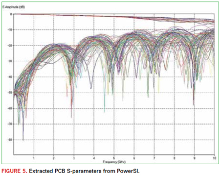
Available technology attacks this daunting problem in a unique manner. Using a patented “hybrid solver” technique, the layout is decomposed into traces, vias, planes and circuits (e.g., for decoupling cap models). These elements are sent off to specifically tuned solvers optimized for these structures, and their results are integrated back together into comprehensive S-parameters. This technique provides nearly full-wave accuracy, while at the same time enables very large-scale problems to be handled in a reasonable amount of time. These S-parameters can be simulated directly in the time domain, or optionally converted into Broadband SPICE models, providing even better time-domain simulation performance (Figure 5).
Simulation Environment
The challenges with regard to simulation environment in the context of power-aware SI fall into several categories: bus modeling, the time-domain simulation itself, and post-processing of results. The bus modeling challenge comes once the models are available for the I/Os, decoupling caps, and passive interconnect. At that point, it becomes necessary to build out or represent the entire die-to-die topology of the bus of interest for simulation. It is generally convenient to do this in a schematic-like environment, where the bus is easily visualized across chip, package, and board fabrics.
There are a few enabling features of a schematic-like environment that facilitate analysis. One of these is hierarchical connectivity, which is in contrast to the “wire-by-wire” connectivity found in traditional schematic-based tools. Wire-by-wire connectivity, in which each individual wire is shown from terminal to terminal in the schematic, works fine with smaller topologies. But as you look to model large groups of coupled signals, together with multiple power and ground connections in each model, this approach quickly becomes impractical. In a hierarchical connectivity approach, only a single connection is shown between models, with the explicit wiring details available one level below. This enables significantly large bus topologies to be easily constructed for analysis (Figure 6).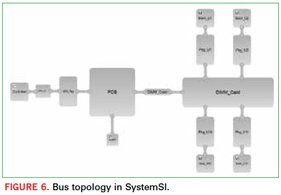
With regard to the simulation itself, it appears this would be straightforward, but there are still some things to consider. SI tools have historically broken down a bus-level problem into multiple piecemeal parts, such as running uncoupled single-line simulations on individual signals to gather delay data, then running other partially coupled subsets of the bus to gather some coupling-related effects, and then trying to combine the results together afterward. (SSO is typically ignored altogether.) This kind of divide-and-conquer approach worked well when the margins were relatively large, but the margins on a modern 1.6 Gbps DDR3 data bus are substantially different from those of the 333 Mbps DDR data buses of yesteryear, when those techniques were commonly deployed.
In hardware, reflections and inter-symbol interference (ISI) do not occur independently of crosstalk or SSO. These effects all happen together, where each affects the other. They cannot be cleanly separated. The simulation needs to much more closely emulate the behavior of the hardware, which boils down to essentially running the entire bus structure in one large simulation. In this manner, all the interplay and interactions between these major effects are captured in the results. The other benefit of this approach is that raw setup and hold measurements can be taken directly, the same way one would measure it in the lab with an oscilloscope.
Post-Processing and Analysis of Results
Once the simulation results are available, the next challenge is to automate the post-processing of the raw waveforms in order to take measurements, generate reports, and close timing. A multitude of measurements are called out per the latest Jedec specifications for DDR memory interfaces. To do this comprehensively, measurements must be taken for each signal, on every cycle. This produces a tremendous amount of data very quickly, so plots of the data are very useful in evaluating the design, as opposed to just generating spreadsheets with many, many rows.
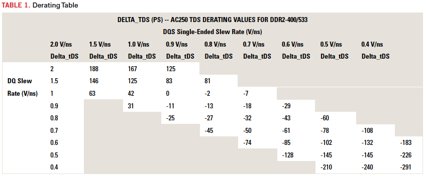
Another key aspect of the post-processing is to automate the derating of setup and hold times (Figure 7). Per Jedec specifications, the slew rates of the signals determine how much more or less setup and hold time is required at the memory, on top of the base setup and hold requirements. What this means for the case of a data bus is that the slew rates of the data and strobe signals need to be automatically measured at each cycle. Then from those two pieces of data, a lookup table provides the incremental setup and hold delta that applies for that cycle, and a final setup and hold margin can be determined, again for that cycle. This needs to be repeated on each cycle for all signals. Again, the amount of data accumulates very quickly, so automation is critical. 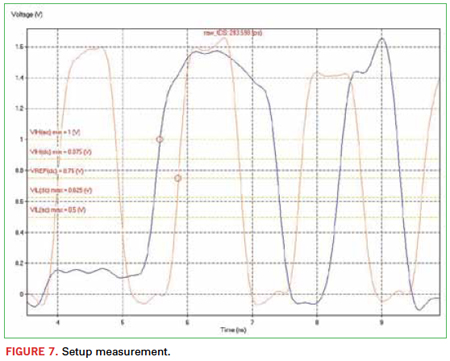
To handle the large quantity of data and close timing, the automated reporting needs to post-process the data and provide intelligent summaries to show critical results, such as:
- Positive setup and hold margins for address/command and control buses, and for data bus “write” transactions at the memory devices.
- Skew requirements are met at the controller for data bus “read” transactions.
- Strobe-to-clock skew requirements are met.
Summary
Moving from an ideal power assumption to a power-aware SI methodology requires some upgrades to modeling and simulation techniques, and is required for adequate SSN characterization of modern memory systems.
A key enabler is power-aware I/O modeling, allowing SSN simulations in minutes on a laptop instead of days on a large server. From the release of IBIS 5.0 and onward, there is an industry-standard way in which this can be done, and tools are available to automate the generation of these models from transistor-level netlists. Demand by systems engineers will quickly drive the broader availability of these I/O models from component suppliers.
Tools to perform efficient interconnect and PDN extraction have been available in the market for a number of years, and are becoming increasingly mainstream for SI applications, as the number of DDR3 and DDR4 design starts increase over time. Simulation environments also require advancement to handle complex bus topologies, comprehensive simulation, and highly automated post-processing to analyze today’s challenging interfaces.
[Ed.: To enlarge the figure, right-click on it, then click View Image, then left-click on the figure.)
Ken Willis is product engineering director, and Brad Brim is senior staff product engineer – High Speed Analysis Products at Cadence Design Systems (cadence.com); This email address is being protected from spambots. You need JavaScript enabled to view it..


