Stepping Out With 0.4mm Pitch BGA/PoPs
Design considerations for moving from 0.5mm pitch to 0.4mm pitch and below.
Package-on-package is a method of stacking components atop one another. Some OEMs use PoP to reduce the board real estate area, particularly for small handheld products and devices. Others are moving to PoP because end-markets demand greater performance in smaller systems and products. In either case, OEMs will find that there’s a game changer going from 0.5mm pitch BGA PoP to the next generation, 0.4mm ultra-fine pitch BGA PoP.
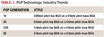
Industry trends say that PoP-populated PCBs will evolve in three stages as shown in Table 1.
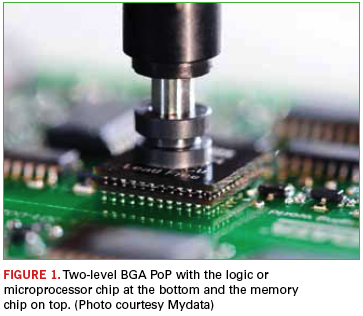
Currently, in some camps, PCB designers are at the first stage using two-level BGA PoP with the logic or µP (processor) chip at the bottom and the memory chip on top (Figure 1). However, there are certain key steps involved in increasing success at the third level. But first, before stepping out with 0.4mm pitch BGA PoP-based PCB designs, it’s important to revisit those rules-of-thumb at the 0.5mm level and above. These rules-of-thumb relate to pad sizes and solder mask openings up to 0.5mm pitch.
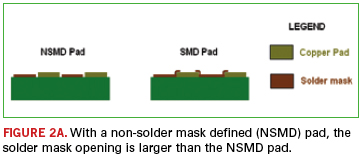
First is to maintain pad size around 85% of the ball size of the BGA. Second is to provide a non-solder mask defined (NSMD) pad whereby the solder mask opening is larger than the NSMD pad (Figure 2a). Typically solder mask is opened to a diameter of around the ball size of the BGA. In this instance, the solder mask is recessed, permitting it to provide stress relief to the NSMD pad during reflow. In short, it creates a protective dam so that solder can go around it.
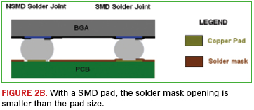
Further, since there are no existing published design guidelines for 0.4mm pitch PoP-based PCBs, be wary of today’s conflicting reports. Issues stemming from these reports deal in large part on PCB pad sizes and solder mask openings. Take, for example, a 0.4mm pitch BGA PCB design using NSMD pad sizes, where in a low-volume run the results were highly acceptable. However, for larger production, this approach produced low yields. By adopting the solder mask defined (SMD) pad approach (Figure 2b), whereby the solder mask opening is smaller than the pad size, better yields and results are achieved. Also, it’s important to note when deploying NSMD pads for 0.4mm and 0.3mm pitch BGA/PoPs, the chances are great of creating bridging between pads due to insufficient solder mask webbing between pads.
Key Factors to Pursue
Since 0.4mm pitch BGA PoP-based PCB design is in its infancy, it is a good idea for the PCB designer to perform preliminary experimental layouts and prototype rounds to get the lay of the design before launching into a full-fledged layout. Rules followed for 0.5mm pitches may not work for 0.4mm cases at high volumes. Typically, ball sizes of 0.4mm pitches are smaller. Reducing the pad size by another 15% may make the solderable area insufficient. Second, using NSMD with 0.4mm parts may cause bridging between adjacent pads. Third, since the pad sizes are so small, and there is no solder mask webbing to provide adhesive strength, it may peel off during reflow or in the field.
Against this backdrop, there are six key factors affecting the reliability of a 0.4mm ultra-fine pitch BGA/PoP-based PCB design. Those are pad design, via-in-pad guidelines, via finish, stencil design, solder paste, and thermal profile.
As suggested, SMD is the pad of choice for 0.4mm pitch. In this case, the pad is created as the same size of the BGA ball. Solder mask opening is around 15% less than the ball diameter. Here, the solder mask laps over the edge of the copper pad to strengthen the connection in a couple ways: One, it strengthens the bonding between the copper and the PCB’s laminate; two, with the copper pad going farther into the solder mask, copper area is larger. That larger copper area provides a greater surface for the PCB laminate to adhere, making the connection twice as strong.
Also, in these designs, traditional BGA dogbone fan out used for larger pitches with extended real estate is not considered at all. Instead, via-in-pad is used, a specialized technique for escape routing fine-pitch BGAs. Before discussing guidelines for use, it’s a good idea to revisit the via-in-pad approach. This escape routing technique involves vias being placed directly on the BGA pads and filled with a conductive or a nonconductive material, which provides a fairly flat surface. Traditionally, silver was used to fill the vias, and a small increase in density was realized so that the designer could route a few more signals on the outer surface. That technique has evolved considerably, and now the materials of choice fall in the nonconductive category. The reason: Vias filled with a nonconductive epoxy perform better because the coefficient of thermal expansion (CTE) is comparable with that of the PCB.
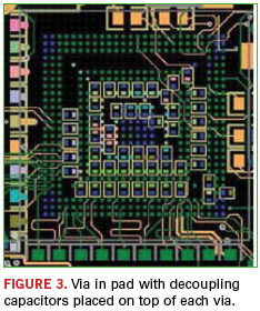
Therefore, the rate of expansion is similar to the board material, allowing for a more reliable joint. Issues like via out gassing and solder voids can be avoided. The same method of filling vias is used on 0.4mm PoP designs. A key point to make is that whenever there are vias below a BGA and available for connection, they should be filled, tented, or capped. Otherwise, they can cause voids and out-gassing during reflow. Also, as shown in Figure 3, discrete decoupling capacitors can be placed directly over the vias on the bottom side. This provides a low inductance path to the power system.
Place and Route
When it comes to 0.4mm pitch BGA PoP, it’s not a good idea to place a BGA on the opposite side of another BGA, which is the typical case in 0.5mm pitch BGA and above. Instead, BGA/PoPs should be placed offset from each other with about 500 mils spacing to maintain board level reliability and ease of debugging on the bench when needed.
Again, since 0.4mm pitch BGA/PoPs are so new, manual routing is recommended over autorouting. Reason: An autorouter is a computer program based on mathematical algorithms and fixated on making connections. It doesn’t think like a human designer. In most instances, using the autorouter results in unusual traces, many unnecessary vias routed and many unnecessary loops.
In effect, the autorouter creates more vias than are required, thus reducing the reliability of the final assembly. Also, those extra vias add discontinuities if the design calls for certain impedance requirements. Typically, impedance is based on the geometry of the connection from driver to receiver. Hence, that impedance path needs to be uniform. Whenever there is a via, there is a discontinuity in that uniform pad, and impedance changes at that particular moment. Ideally, for a 0.4mm pitch BGA/PoP-based design with high-speed signals, you don’t want a via. Additional vias will cause considerable discontinuities and subsequent ringing and reflections.
While performing the routing, it’s also vital to avoid creating heat sinks. How can a designer inadvertently do this? This occurs when a trace is put on a via or a dogbone fan out is performed from a via that’s almost the same size as the pad. The result is the traces and vias pull heat away from the BGA/PoP and cause issues during assembly. In another example, copper pour is placed over BGAs. This may happen when there are multiple power/ground pins on the device. During assembly, this arrangement will sink the heat during reflow and cause cold solder joints, resulting in opens or intermittent connections.
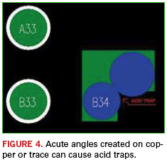
Also, in the realm of routing, acute angle traces should be avoided when connecting BGA pads, as they could result in acid traps. Acid traps are acute angle areas or small areas where etching chemicals get stuck, and eventually, those small chemicals eat away the traces and intermittent connections result (Figure 4). Finally, the designer should design with metric units rather than English for fine-pitch BGA devices and PoP. This will not only increase accuracy, but will also avoid requiring four decimal places of accuracy when converting from micrometers to mils.
Team Effort
There’s always talk about working together to successfully complete a project. But in the case of 0.4mm ultra-fine pitch BGA/PoP-based PCBs, there is no question it is essential that the PCB designer, fabricator and assembler work in unison, with the designer taking the lead. The PCB designer must maintain regular discussions with the fabricator to understand its capabilities, such as determining whether it can handle certain minimum hole size aspect ratios. Part of that dialogue includes understanding the spacings for a high-speed design’s impedance control traces, and knowing the chosen substrate material’s capacity to handle those requirements.
Furthermore, the designer must have a good handle on a fabricator’s manufacturing limits. Those can be divided into three categories: standard technology, high-yield, and engineering development. The first refers to a fabricator’s capability, for example, 5 mil traces and spacing, which is a midrange capability for most board shops today. For mass production, high yield is typically 8 mil lines and spaces. (These numbers are relative, so for some fabricators, 10 mils will be high yield, while 8 mils might be typical for others.) Third, there’s the engineering development category. This deals with a fabricator’s highly advanced capabilities, which fall into the 2.5 mil traces and 2.5 mil spacing class.
The layout designer must also know the assembler’s capabilities, such as the minimum pitch that assembler can work with. Either it can or cannot perform 0.4mm ultra-fine pitch BGA/PoP PCB assembly. If it is building 0.4mm pitch, what kind of solder paste are they using? Are they following manufacturer’s recommendations on the reflow profile? The designer must also have discussions with the paste manufacturer to ensure the right pad sizes are associated with the right solder paste.
Avoiding warpage is another key area demanding close interaction between the designer and assembly. By not paying special attention in this area, excessive warpage can result in bridging, solder slumping, head in pillow, or opens.
PoP is an emerging technology, and will be utilized more as the industry gears toward further miniaturization of the existing technologies. Do not assume that the same techniques that work for larger versions will necessarily scale to the smaller ones.
Syed W. Ali, C.I.D+ is a PCB layout engineer at Nexlogic Technologies (nexlogic.com); This email address is being protected from spambots. You need JavaScript enabled to view it..


