The Proposed IEEE Test Standards

A host of new specifications aims to overcome coverage issues brought on by high-speed circuits.
The influx of high-speed signals on boards, and the challenge to the test environment, has invigorated interest in limited access methodologies such as boundary scan and built-in self-test (BIST). The industry is gearing toward adopting key initiatives to IEEE standards, so as to be able to help resolve these test challenges. The following are the proposals to extend IEEE Standard 1149.1 boundary scan capability into embedded testing, as well as the BIST currently in use by OEMs in the semiconductor and board design areas.
IEEE P1687
The challenge. Board assemblies increasingly are populated with high-speed semiconductors and memory in the GHz range. As a result, placing testpoints on the PCB traces is nearly impossible, as it would degrade signal integrity. Without these testpoints, manufacturers will no longer be able to use ICT to capture defects such as opens, shorts and wrong component values. In turn, this would increase test and overall manufacturing costs.
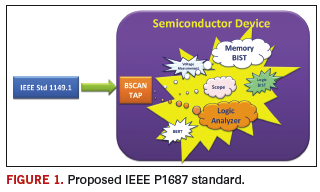
The proposed solution. OEMs and EMS providers are well aware of these challenges. Their need for a viable solution paved the way for the surge in interest in the IEEE P1687 standard, also known as Instrument JTAG or iJTAG. The objective of iJTAG is to develop a method and rules to access the instrumentation embedded into a semiconductor device without the need to define the instruments or their features using IEEE Standard 1149.1. The proposed standard would include a description language that specifies an interface to help communicate with the internal embedded instrumentation and features within the semiconductor device (Figure 1).
The purpose of the P1687 or iJTAG initiative is to provide an extension to IEEE 1149.1 specifically aimed at using the TAP to manage the configuration, operation and collection of data from this embedded instrumentation circuitry.
The benefit. With the proposed IEEE P1687 standard, test equipment providers will be able to access the embedded instruments in the semiconductor devices for testing purposes. At the same time, electronics manufacturers will be able to regain test coverage with minimal cost impact by integrating this solution into their current test process. Here are some ways in which P1687 can be implemented on the manufacturing floor:
1. Integrated into existing ICT.
2. ICT system > P1687 test solution.
3. P1687 test solution > functional test.
4. Integrated into existing functional test.
Among the possible implementations for P1687, integration into the ICT system would most benefit manufacturers, as the majority of high-volume companies use ICT to screen structural defects. With this implementation, EMS companies would be able to increase the value of their ICT and avoid a costly investment in another system to cover both the analog and digital defects of the assembly.
IEEE P1581
The challenge. One of the most common devices today is Dynamic Data Rate (DDR) memory, which can be found on everything from netbook motherboards to a larger high-end server and telecommunications boards. The challenge in testing memory devices lies in the high clock speeds for DDR memory, which now run in the GHz range. Again, with such clock speeds, testpoints would no longer be viable. The lost coverage means failures could only be captured after ICT, where finding defects and repairing them would be five times more costly.
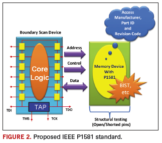
The proposed solution. The proposed IEEE P1581 (Figure 2) aims to develop a standard method for testing low-cost, complex DDR memory devices, which would be able to communicate through another semiconductor device with an IEEE 1149.1 boundary scan capability. Presently, even if DDR memory devices adopt the IEEE 1149.1 boundary scan standard, this is still not a feasible test, as it will require the addition of the four mandatory TAP pins to the DDR device, which would add to the devices’ complexity and cost. P1581 would provide the protocol to access the test mode within the memory devices, without the need for dedicated test pin requirements. The defined standard for this new test technology would enable each vendor to create its own method for implementing test hardware functionality in memory devices. It guides them on the necessary implementation rules for access and exit test modes. In contrast to IEEE 1149.1, this standard provides a static test method and requires fewer test pins. The standard would also allow implementation of P1581 on other semiconductor devices besides memory devices.
The benefit. P1581 would help the DDR memory vendor to enable its memory devices to communicate with boundary scan-enabled devices. Manufacturers would regain the test coverage on DDR memory that even current standalone solutions like 1149.1 are finding hard to run with any good measure of stability due to high clock speeds.
IEEE 1149.8.1
The challenge. High-speed differential signals, commonly known as SerDes (serial/deserializer) are reason to remove testpoints on assemblies. ICT has seen innovations to regain test coverage on connectors and devices connected to boundary scan devices without the need for testpoints by using a combination of boundary scan devices as signal driver and a noncontact signal sensing or vectorless sensor plate to detect opens and shorts on connectors, sockets and semiconductor device pins. However, this solution still falls short of being able to provide 100% coverage on differential signals. An example of failure escaping detection is when both differential signals (Tx+ and Tx-) are open, but the detected measured value of vectorless sensor plate will still be the same when both signal pins are properly soldered (Figure 3).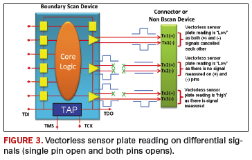
The proposed solution. IEEE 1149.8.1 entails a selective AC stimulus or differential signals, which when combined with noncontact signal sensing or a vectorless sensor plate, will allow testing of the connections between devices that adhere to this standard and circuitry elements such as series components, sockets, connectors and semiconductor devices that do not implement IEEE 1149.1 standards.
This standard specifies extensions to IEEE 1149.1 that define the boundary-scan structures and methods required to facilitate boundary scan-based stimulus of interconnections to passive and/or active components. This standard also specifies Boundary Scan Description Language (BSDL) extensions to IEEE Standard 1149.1 required to describe and support the new structures and methods (Figure 4).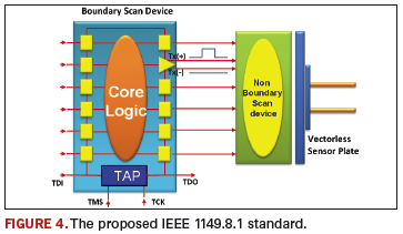
The benefit. IEEE 1149.8.1 would enable selective AC stimulus generation that, when combined with noncontact signal sensing, would allow testing of signal paths between devices adhering to this standard and passive and/or active components. The biggest benefit of 1149.8.1 is that there is already a working solution currently implemented in some ICTs using a noncontact signal sensing or vectorless sensor plate that detects open/shorted pins on non-boundary scan devices and connectors connected to boundary scan devices.
IEEE 1149.7
The challenge. Assemblies, especially those used in consumer products, are pressured by shrinking form factors. In recent years, we have seen implementation of multi-core system-on-chip (SoC), multi-die packages on system-on-package (SoP), and package-on-package (PoP) devices. All these technologies pose new challenges when it comes to manufacturing test due to limited testpoints and higher speed. This is causing existing manufacturing test systems to lose test coverage, even with the implementation of IEEE 1149.1.
The proposed solution. IEEE 1149.7, also known as compact JTAG or cJTAG, is compatible with the traditional IEEE 1149.1 (JTAG) standard to provide an enhanced test and debug standard that meets the demands of modern systems. One unique feature of 1149.7 is the reduced pin count interface for the test access port (TAP) interface; it uses a two-wire interface, versus the traditional 1149.1 four- or five-wire TAP interface. Since IEEE 1149.7 is compatible with 1149.1, this proposed standard also permits four- or five-wire implementation (Figure 5).
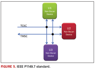
With the adoption of a two-wire interface on IEEE 1149.7, devices on the IEEE 1149.1 standard will benefit from this, as it makes it easier for boundary scan to be implemented on complicated new package technologies such as SoC, SoP and PoP, which does not implement 1149.1 boundary scan chain using the standard four or five-wire TAP interface.
The benefits. IEEE 1149.7 would enable easier implementation of IEEE 1149.1 for SoC, SiP and PoP. IEEE 1149.1 implementation is limited to boundary scan chains, as it requires the connection of every TAP interface of every boundary scan device targeted for testing. In comparison, IEEE 1149.7 would simplify this by enabling a star architecture (Figure 5) more appropriate for SoCs, SiPs and PoPs. When used on SoCs, 1149.7 would enable testing and debugging of each core or chip in the package, using boundary scan in a single 1149.7 two-wire interface. This implementation is also possible on multi-die SiPs or PoPs. A key advantage of 1149.7 is that it can be implemented on through-silicon vias that would link each die through a via that connects the 1149.7 interface on each die to one another.
How successfully these proposed standards are adopted on the manufacturing floor depends on how well they will fit into the existing manufacturing test systems such as ICT, manufacturing defect analyzers and functional testers without impacting throughput, and while regaining maximum test coverage no longer available on the older testers. Another important factor will be the cost of the tools and their implementation.
Bibliography
1. Bill Eklow and Ben Bennetts, IEEE P1687 (IJTAG) Draft Standard for Access and Control of Instrumentation Embedded Within a Semiconductor Device, ETS 2006 embedded tutorial.
2. IEEE P1687 Working Group, http://grouper.ieee.org/groups/1687/.
3. IEEE P1581 Working Group, http://grouper.ieee.org/groups/1581/.
4. P1581 Working Group, “An Economical Alternative to Boundary Scan in Memory Devices,” January 2007.
5. IEEE 1149.8.1 Working Group, http://grouper.ieee.org/groups/atoggle/.
6. Adam Ley, “New 1149.7 Enhances 1149.1 Test Access Port, Maintains Compatibility for Boundary Scan,” Asset Connect, 2009.
Jun Balangue is technical marketing engineer at Agilent Technologies (www.agilent.com); This email address is being protected from spambots. You need JavaScript enabled to view it..


