Fluid Dynamic Simulation for Cool Designs
Published: 07 August 2009
by Robin Bornoff
Computational fluid dynamics-based simulations that examine temperature and heat flux can help engineers make better thermal management decisions.
Simulation methods that provide predictions of thermal behavior for an electronics system are many and varied. One characteristic shared by these methods is the prediction of temperatures at many locations between heat sources and the cool ambient temperature. Relating the component temperatures (i.e. heat sources) to their maximum-rated temperature will determine thermal compliance.This observational approach to simulation is valid but, by further examining other outputs, an understanding of why the temperatures are what they are is possible. With this additional knowledge, more-informed design decisions can be made to resolve potential thermal design flaws.
Computational fluid dynamics (CFD) is a software-based simulation technology that enables the prediction of various physical properties at literally hundreds of thousands of discrete locations in and around an electronics system. Pressure, velocity and temperature values are predicted in the air, while temperature and heat fluxes are determined within solid materials. Such a wealth of data would be impossible to obtain experimentally. The following two examples highlight how, by examining not only temperatures but also heat flow paths, one specifically can learn why a thermal design is underperforming or over designed.
Thermal Vias Carry Heat Down and Out
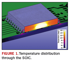
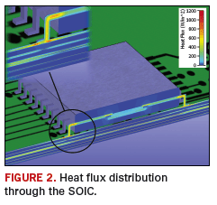
The first example evaluates a ruggedized design in which a printed circuit board (PCB) is wedgelocked inside a sealed enclosure, providing a conduction-cooled thermal environment. A good thermal design would have the heat leaving the components, conducting down to the internal copper-molybdenum-copper stiffening layer in the PCB and out through the wedgelock to the heatsinking fins on the outside of the enclosure. A 44-pin small outline integrated circuit (SOIC) package is powered at 2.0 watts, making it the most thermally critical on the board.The temperature results of an initial CFD simulation are shown in FIGURE 1. The temperature plot indicates a junction temperature of 142.8° C, with the temperature reducing as the heat spreads throughout the package. It is the equivalent heat flux plot shown in FIGURE 2, however, that provides the greatest insight. Heat flux is defined in terms of W/in2 and can be considered somewhat analogous to current density. It clearly shows the dominant paths the heat follows as it leaves the package, unlike the temperature plot where such distinctions are not observed. Heat is seen to leave the die, through the leadframe and along the top signal layers. Some heat does conduct down to the internal-stiffening layer as intended, but the intermediate, thermally resistive dielectric layers create a pronounced thermal break.
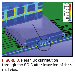
There are several ways to remedy such a heat flow path discontinuity. The first is to add thermal vias directly under the pads, linking the present heat flow path directly to the innerlayers. This would be difficult to achieve from a routing perspective. An alternative is to attempt to link the die directly with the internal layers. This is achieved in two stages. First, change the package style to an exposed pad SOIC, which is soldered onto a matching land on the PCB. Secondly, include an array of thermal vias under the land that connects down to the stiffening layer. FIGURE 3 shows the resulting heat flux plot for this configuration. In this example, the junction temperature rise decreases by 41.4%, down to 88.6° C, now below the maximum rated junction temperature of 100°C.
It is commonly accepted that for natural convection-cooled (no fans moving the air) and conduction-cooled environments, adding more copper to the board will help the thermal performance. Following this advice and applying it to the previous example might have led to a decision to simply increase the thickness of the stiffening layer. By understanding the concept of a continuous, dominant heat flow path to the cooling ambient, one can appreciate the more effective approach of using thermal vias and an exposed pad. In fact, once a continuous heat flow path has been designed in, one can start to further reduce the overall resistance by adding as much copper as possible along that path, including the internal layers.
Before moving on, it’s worthwhile to elaborate on the differences between electrical and thermal resistivities. The difference between the electrical resistivity of copper and FR-4 is approximately 20 orders of magnitude. The equivalent difference between the thermal resistivity (taken to be the inverse of the thermal conductivity) is only 3 orders of magnitude. It is because of these ratios that the electrical current travels exclusively within copper, while the heat tends to follow the copper and to spread through the FR-4. The apparent breaks in the heat flow paths in Figure 1 do not mean that heat is unable to leave the system to the ambient. Instead, it is forced to spread and to pass through the more thermally resistive FR-4 regions on its way out. This causes an increase (build up) of temperature back down the heat flow path and ultimately to the source.
CFD Analysis Helps a Heat Sink Lose Weight
The second example contains probably the most common of all electronics cooling solutions: a heat sink. The name is somewhat misleading in that a heat sink does not provide a pit into which the heat is magically absorbed, thereby removing it from the system. The heat sink does, however, play a critical role in connecting the heat sources with the cooling ambient air by decreasing the thermal resistance from the package surface to the ambient air. Conductive thermal resistance is formally defined as:
where R is the thermal resistance (K/W), δ is the material length through which the heat passes (m), k is the thermal conductivity of the material (W/mK) and A is the area through which the heat passes (m2).
Compared to a bare component surface, the heat sink results in a decrease in R due to the fact that it provides a much larger cooling area, (A). This “area extension” far outweighs the fact that the heat has to pass a certain distance (δ) through a material with thermal conductivity (k).
For a given volume, a heat sink takes heat from a point source (or a series of point sources) and spreads it to a large surface area, where air then convects it away. Heat sinks have two main parts, a base and a series of fins. The base spreads the heat sideways to the base of each fin. The heat then conducts up only the fins having a large surface area in relation to their volume (they are long and thin).
One might think that having as many thin fins as possible along the base would be the most optimal design; however, the smaller the air gap between the fins becomes, the less likely it is that air will be able to squeeze through to convect the heat away. Ultimately, this traps stagnant air that, unlike moving air, is very thermally resistive. Alternatively, using too few fins decreases the surface area and detracts from the beneficial effect of the heat sink.
A good heat sink thermal design is a trade-off between thermal effectiveness, weight and cost. This is the basis of the second example. A power supply unit has a single fan blowing air through a large heat sink that has 10 TO-220 power invertors. These invertors dissipate 9.5 W each and are connected to the heat sink base. Each inverter has a maximum-rated junction temperature of 100° C, and one of the design goals is to minimize the total mass of the unit.
An initial CFD thermal simulation of the system indicates that each inverter is thermally compliant, with a maximum junction temperature of 93.3° C. By examining the heat flux distribution within the heat sink, it is possible to identify, and perhaps eliminate, parts of the heat sink that are not contributing to heat removal. FIGURE 4 shows the distribution of heat flux on a plane at the mid-height of the fins, and FIGURE 5 shows this through the middle of the heat sink. The heat flux colors are clipped above a maximum and below a minimum value for clarity. The periphery of the heat sink, including the upstream and downstream ends of the fins and the far left and far rights fins, does not receive much heat because of low heat flux values in those areas.
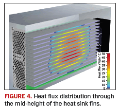
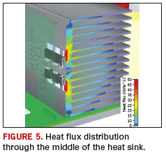
In theory, these sections of the heat sink could be removed without unduly compromising thermal performance. This is investigated in a second study in which the heat sink length and fin height are reduced by 10%, and the two outermost fins are removed altogether. The maximum junction temperature increases slightly to 94.4° C, but more importantly, the total heat sink mass is reduced by nearly 30%.
Conclusion
Whereas generalities such as “more copper in a PCB makes things cooler” and “the bigger the heat sink, the better” are often valid, a greater understanding of heat loss paths through a series of thermal resistances enables more refined conclusions. Thermal design decisions and remedial actions can be applied effectively and implemented with little risk of failure.The necessary understanding can be gained by examining both the temperature and the heat flux results of a CFD-based simulation. Whereas temperature alone enables an observational method of determining thermal compliance (is it too hot?), heat flux simulation explains why the temperature is what it is. PCD&F
Robin Bornoff is the FloTHERM and FloVENT product marketing manager for Mentor Graphics Corporation.


