Effective Use of Split Planes
Published: 02 July 2009
by Dr. Michael L. Steinberger

Split planes affect ground currents, making it difficult to determine the impact on design performance without first knowing where the ground current is going.
The question is whether or not one should use split planes when designing a printed circuit board (PCB). On one side, PCBs tend to have many separate power domains, either because different devices on the board use different supply voltages or because sensitive devices such as clock distribution devices should be isolated from the rest of the board by three terminal power regulators. On the flip side, modern PCBs tend to have a lot of high-speed serial channels on them, and splits in the power planes can disrupt the propagation of these signals or cause electromagnet interference (EMI) problems.The short answer is: If the design can meet performance requirements with split planes and split planes will reduce product cost, use them. Otherwise, don’t.
The cost part of this statement is easy enough to evaluate, but the performance part is a bit harder. The impact of split planes on performance is not necessarily well understood, so it can be hard to decide whether or not that impact is acceptable. The underlying difficulty is that the split affects the ground currents, and it’s not always clear where the ground currents are going.
The purpose of this article, therefore, is to describe where the ground currents are actually going, offer estimates for the affects of these ground paths and suggest what types of performance impacts should therefore be considered.
What’s the Problem?
Before embarking on a discussion of ground current paths, we should first state the ways in which we expect ground current to affect performance. There are three such effects: signal path reflections, crosstalk and EMI.A split plane will introduce a series impedance in the ground path, thereby locally increasing the impedance of the transmission line and causing reflections. Signal path reflections are a concern because if the reflection coefficient when crossing a split in a plane is high, then the signal will be distorted. In particular, a digital signal may be distorted to such an extent that the data cannot be recovered accurately. Similarly, a clock signal may be severely attenuated, possibly resulting in loss of clock at the far end.
Crosstalk at a split plane can occur because the split introduces a common ground impedance in the ground path for nearby signals. If this crosstalk is high enough, it can cause errors in digital signals and phase noise in clock signals.
Split planes cause the ground currents to deviate from their desired path. If some of the ground currents are deflected to the edge of the PCB, they could cause radiation, which could be detected as EMI at the system level. This radiation must not become so high that it causes the system to fail its EMI requirements, and EMI fixes at the system level tend to be expensive.
Decaps or Not?
Years ago, the conventional wisdom was that the ground currents around split planes somehow made their way back to the decoupling capacitors, but this statement is only valid at tens of MHz. At higher frequencies, the ground currents can find other paths that are lower impedance.To be precise, it is possible for a decoupling capacitor to be effective if its distance from the signal trace is less than a quarter wavelength at the maximum frequency of interest. One of the experiments we ran was to measure the transmission loss of a structure with and without ground vias completing the ground path. The results are shown in FIGURE 1 and FIGURE 2, for ground vias placed at two different distances from the signal conductor.
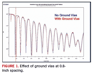
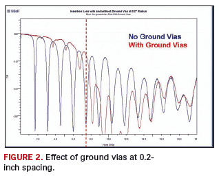
In Figures 1 and 2, a red dashed line indicates the quarter wavelength frequency for the via spacing. Comparing the blue curves (without ground vias) to the red curves (with ground vias), it is clear that below the quarter wave frequency, the ground vias had a very noticeable effect, whereas above the quarter wave frequency, they had essentially no effect at all. Considering that the best one could hope for from a decoupling capacitor is that it would look electrically like a ground via at high frequencies, the quarter wave principle applies to the decoupling capacitors as well.
One could, of course, place decoupling capacitors at a suitable spacing along the split in the plane. For example, for a 3-Gb/s design, one could place a capacitor stitching the split together every three-quarters of an inch. In order to be effective, they would have to be high quality capacitors on well-designed mounting pads. But then, high quality decoupling capacitors cost money, and wasn’t the whole premise of a split plane that it would save money?
Split Plane with Microstrip: A Slot Antenna
Suppose that a microstrip crosses a split in a ground plane, as shown in FIGURE 3. One would suspect that in this case, the split in the ground plane would result in a completely open circuit, with all of the ground current reflected back toward the signal source. At DC, that’s clearly the case; however, at higher frequencies, other things can happen.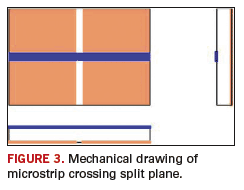
The fact of the matter is that some RF engineers call the structure in Figure 3 a slot antenna, and they build them on purpose to efficiently couple the energy on the microstrip at some frequency into the atmosphere. So, at some frequency, the ground impedance across the split plane could very likely be comparable to the impedance of the transmission line, and some appreciable signal energy could flow across the split.
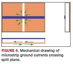
The ground currents might look something like FIGURE 4. In general, ground currents will flow on both the top and the bottom of the ground plane, and they will be anti-symmetric with respect to the split.
Split Plane on Top of Continuous Plane: Radial TEM Modes
Suppose that the structure in Figure 3 is augmented with another ground plane underneath the split, as shown in FIGURE 5.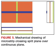
The adjacent plane alters the physics of the structure substantially. For example, there will be a considerable capacitance between each side of the split plane and the ground plane underneath it. At low frequencies, the capacitance on each side will behave as a lumped capacitance, and the two capacitances are connected in series by the adjacent ground plane. If the adjacent plane is close to the split plane and there is a lot of overlap area on each side of the split, the ground impedance will be quite low, and most of the ground current will follow that path. This situation is illustrated in FIGURE 6.
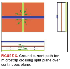
At higher frequencies, the ground plane capacitances will cease to behave as lumped circuit elements, and there will be frequencies at which they resonate as open circuits. These resonances and the coupling to them can be analyzed very effectively on the basis of radial transverse electromagnetic (TEM) waves1 that describe both circumferentially symmetric TEM waves associated with a single ended via and circumferentially varying radial TEM waves associated with differential vias. The radial TEM waves associated with the structure in Figure 5 will be antisymmetric, with respect to the split, and will be of the circumferentially varying type.
Split Plane with Stripline: Weak Radial TEM Modes
If another ground plane is added to the structure in Figure 5 on the other side of the transmission line, as shown in FIGURE 7, then the transmission line becomes stripline rather than microstrip.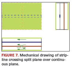
One clear advantage of this structure is that only half the ground current needs to cross the split plane, thus cutting the effect of the split in half. The half of the ground current that still has to cross the split will follow the path shown in FIGURE 8.
One remaining detail is that the fields at the split will not be completely symmetrical, resulting in a small voltage between the split plane and the upper ground plane. This will generate antisymmtrical radial TEM waves similar to those depicted in Figure 6, only with much smaller amplitude. These waves should still be accounted for in the PCB’s EMI solution.
Split Plane with Differential Pair
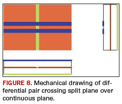
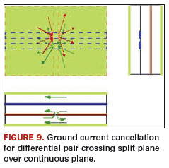
Any of the above structures could be used with a differential pair rather than a single ended transmission line. For the sake of clarity, we will show a differential version of the structure in Figure 5.When the differential pair is driven in differential mode, the ground currents nearly cancel each other out, with the degree of cancellation dependent on the number of wavelengths by which the two traces are separated. For separations up to one-tenth of a wavelength, the cancellation of ground currents is quite good, and there is still some useful cancellation at a quarter wavelength. Most differential pairs have a much smaller spacing than that. FIGURE 9 depicts this cancellation. In short, a split plane will have very little effect on a different pair.
Effect on the Design
An intuitive understanding of the ground current path, as presented above, can help predict the effect of a split plane on performance. The following major considerations need to be factored into the equation.Signal Path Reflections
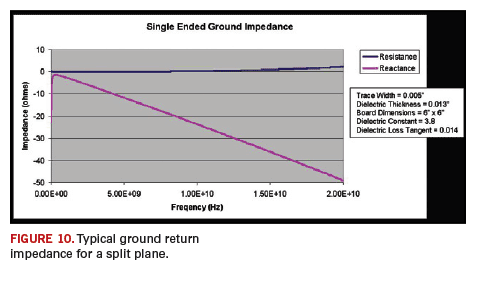
Given the ground current paths described, one would expect the split plane to introduce a series impedance in the ground path. However, if there is another plane covering the split, as shown in Figures 5 and 6, then the capacitance between the planes will complete the ground return path; and if that capacitance is fairly large, then the discontinuity introduced into the transmission path needn’t be too serious.Of course, this simple view of inter-plane capacitance will break down at higher frequencies, and a more complex analysis is required. We can get a decent estimate of this impedance by using the radial TEM wave concepts described previously. In this case, a circumferentially varying radial TEM wave is needed to approximate the current path. If reflections from the edges of the PCB are ignored, then the ground return impedance for a representative set of PCB dimensions is shown in FIGURE 10. When reflections from the edge of the board are taken into account, this impedance goes down for most frequencies but increases at the resonant frequencies of the plane structure.
In the case of differential traces, the radial TEM waves from the two sides of the differential pair tend to cancel each other out, and the effect of the split on signal propagation is negligible.
Crosstalk
If two parallel signal traces cross a split, then each will generate radial TEM waves, and those radial TEM waves will cross paths. The net result is a common ground impedance. The closer the signal traces are to each other, the stronger the radial TEM waves will be when they overlap and the greater the common ground impedance will be. FIGURE 11 shows an estimate of the crosstalk coupling for single-ended traces as a function of separation for a typical set of PCB dimensions.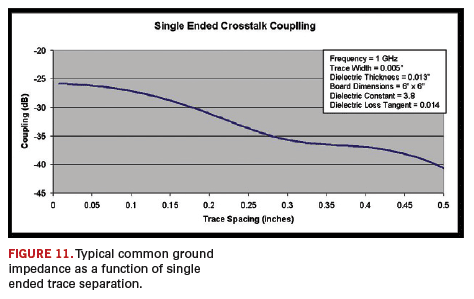
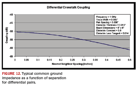
If differential traces are used, then the radial TEM waves tend to cancel each other out, making the wave amplitude where the TEM waves overlap much lower. Whatever common ground impedance remains, however, behaves very much like the coupling between two single-ended traces. Think of this as the coupling between the nearest trace of one differential pair to the nearest trace of the other differential pair. FIGURE 12 shows an estimate of the crosstalk coupling as a function of separation for a typical set of PCB dimensions.
Electromagnetic Interference
First of all, we noted that microwavers call a split that is not covered by another plane a slot antenna. Antenna ... radiates – maybe not a very nice thing to do to your EMI engineer.For splits which are covered by another plane, there are still going to be radial TEM waves propagating between the planes and reflecting back at the edges of the planes. Since the spacing between planes is relatively small, there isn’t going to be a lot of radiation, but there will be some. H. W. Ott’s classic text2 suggests stitching ground vias along the edge of the board to suppress the radiation. Ott’s explanation is correct, and the suggestion is a good one. Ground vias spaced more than a quarter wave away from a given source of ground current have relatively little effect, while vias that are within a quarter wave are quite effective. That explanation applies to ground vias stitched along the edge of the board as well.
Overall Recommendations
- Don’t use microstrip for any high frequency signal, ever. Power supplies and control signals are permissible.
- For each split, provide a complete overlap with as much area as possible on adjacent ground planes.
- Stitch the edges of the board with ground vias less than a quarter wavelength apart at the maximum frequency of interest.
- If single ended traces cross a split in the ground plane, try to minimize crosstalk by spacing them as far apart as possible where they cross the split. A spacing of at least ten times the ground plane spacing is strongly recommended.
- Whenever possible, use differential traces to cross a split plane. PCD&F
REFERENCES
1. C. Ding, D. Gopinath, D. Scearce, M. Steinberger, D. White, “A Simple Via Experiment,” DesignCon2009.2. H. W. Ott, Noise Reduction Techniques in Electronic Systems, second edition, John Wiley and Sons, 1988.
Dr. Michael L. Steinberger is chief architect, Serial Link Analysis Products, Signal Integrity Software, Inc.; at SiSoft; This email address is being protected from spambots. You need JavaScript enabled to view it..


