Tackling the Copper Wrap Plate Requirement
Published: 01 July 2009
by Rajwant Sidhu, Ph.D.

Wrap plating improves reliability of via structures, but conventional techniques increase surface copper thickness, limiting HDI and other fine-line designs.
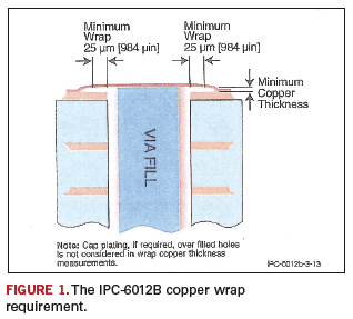
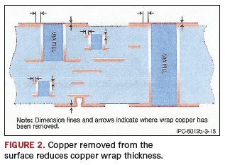
Multilayer printed circuit board (PCB) production is a constantly evolving, increasingly complex interplay of processing techniques, customer demands, design rules and product specifications. Many times, new processes are added to meet certain demands but are not easily and fully integrated into the existing process web. The IPC added a copper wrap plate requirement to the IPC 6012B specification, requiring that copper plating, from the filled plated hole, continues around the knee of the hole and onto the surface. This requirement was introduced to improve reliability and reduce failures due to separation between surface features/caps and the plated hole-wall. The increased surface copper thickness, due to copper wrap plate, posed additional challenges for both the PCB designer and the fabricator.IPC-6012B specifies that copper wrap plating shall be continuous from the filled plated hole onto the external surface of the plated structure and extend by a minimum of 25 microns (984 microinches) where an annular ring is required. FIGURE 1 shows this requirement. FIGURE 2 shows that any reduction of wrap plating by processing (sanding, etching, planarization, etc.) that results in insufficient wrap plating is not allowed.
PCBs that require filled plated holes are less prone to thermally induced separations between surface features and the plated hole-wall with copper wrap plating. However, conventional wrap plating increases surface copper thickness due to copper wrap build up over the entire surface of the copper. This increased thickness makes it difficult for fabricators to produce PCBs with higher density and finer lines. The IPC specification for Class 2 requires a minimum of 0.000197-inch continuous copper wrap from hole-wall onto the external surface of a plated structure, and IPC Class 3 requires a minimum of 0.000472-inch continuous copper wrap. The challenge is meeting these specifications while still building high reliability PCBs without compromising the design rules that are required to fabricate HDI designs.
TABLE 1 illustrates the effects of copper wrap on fabrication design rules for line width and space. For example, starting with three-eighths of an ounce of copper foil, this particular fabricator shows a space requirement of 0.0035 inch to produce a 0.003-inch feature for designs that do not require wrap plating. In the same example, if two copper wraps are needed, the space requirement increases from 0.0035 inch to 0.007 inch for Class 2 and from 0.0035 inch to 0.0085 inch for Class 3 (standard builds).

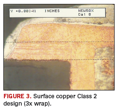
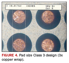
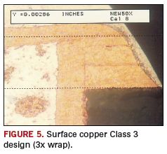
Fabrication processes, such as lamination, plating and planarization, have an effect on the consistency of copper wrap plating thickness across a PCB panel. Variations from these processes force fabricators to plate more copper on the external surface of filled plated holes than required by IPC specification 6012B. This is done to insure minimum copper wrap is maintained across the entire panel, which further reduces the capability to produce fine lines and spaces. FIGURE 3 shows copper wrap plating for a filled plated hole with three Class 2 wraps. The total surface copper thickness of three copper wrap plates and initial copper foil is 0.0014 inch. This copper thickness is etched to create the surface copper features. FIGURE 4 shows the top of the BGA pad features illustrated by the cross-section view in Figure 3. Starting with an imaged pad size of 0.022 inch, the resulting finished diameter of the pad is 0.0176 inch, as measured from the top. Likewise, FIGURE 5 shows copper wrap plating for a filled plated hole with three Class 3 wraps. The total surface copper thickness of three copper wrap plates and initial copper foil is 0.0029 inch. This copper thickness is etched to create the surface copper features. FIGURE 6 shows the top of the BGA pad features as illustrated by the cross-section view in Figure 5. Starting with an imaged pad size of 0.022 inch, the resulting finished diameter is 0.0137 inch, as measured from the top.
Tackling the Wrap Plate Challenge
Flat-wrap1 technology provides a novel solution to the design and manufacturing issues related to copper wrap requirements, offering reliability without limiting fabrication capability. The new technology also has the benefit of verifying the wrap thickness without coupon correlation and destructive cross-sectioning analysis. One can control the copper wrap thickness by changing the starting surface copper thickness. Diagrams for comparison of the conventional process and the new process can be seen in FIGURE 7 and FIGURE 8. This design required three sequential wrap plate cycles. Note the difference in copper surface thickness between the conventional process and the new technology.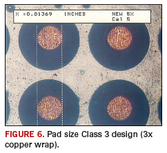
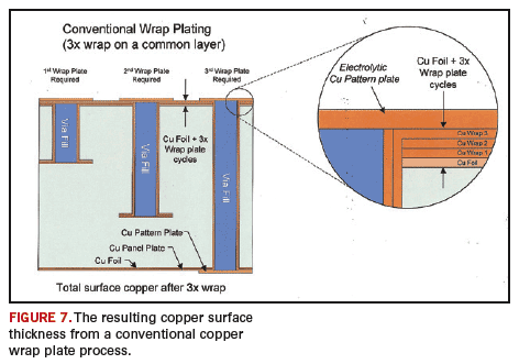
TABLE 2 shows theoretical surface copper buildup for multiple wraps, comparing conventional Class 2, Class 3 and Class 3 with the new technology. With a conventional wrap process, the surface copper thickness increases with every wrap plate cycle. With the new technology, the surface copper thickness remains the same, regardless of the number of wrap plate cycles.
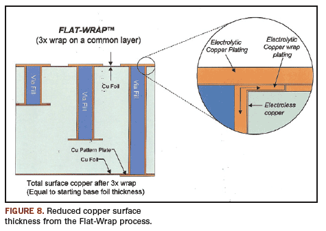
TABLE 3 shows a comparison of surface copper thickness and finished pad size starting with one-half ounce of foil and an imaged pad size of 0.022 inch for Conventional Class 2, Class 3 and Class 3 with the new technology. The surface copper thickness is critical, as this thickness of copper is etched to create copper surface features.

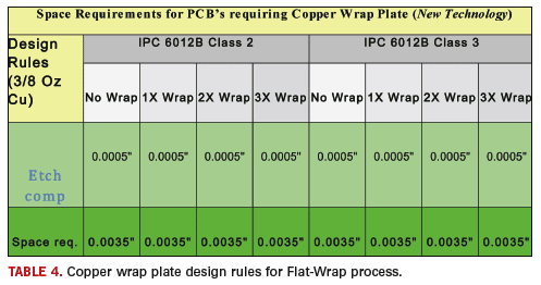
TABLE 4 illustrates the benefit on fabrication design rules with copper wrap requirements. Starting with three-eighths of an ounce of copper foil, this particular fabricator shows a space requirement of 0.0035 inch to produce 0.003 inch features for designs that do not require wrap plating. Starting with the same surface copper thickness, the space requirement remains the same with the new technology, regardless of the number of wrap plate cycles.

Description of Flat-Wrap Technology
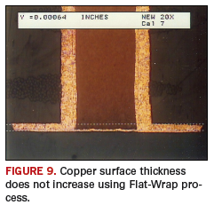
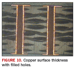
In the Flat-Wrap process, the copper wrap plate is created with an innovative approach that allows verification of the wrap plate thickness without any destructive cross sectioning. The copper wrap plate is created by selectively recessing or removing the surface copper around the filled plated holes. The plating from the hole-wall continuously wraps onto the surface of the substrate to substantially the same thickness height of the surface copper. This feature allows verification of the wrap plate thickness without destructive cross sectioning.The wrap thickness can be measured by using a surface copper probe. This process also enables fabricators to verify wrap thickness across the entire panel and for each panel within a lot. FIGURE 9 shows that the wrap plate thickness is essentially the same as the initial starting thickness of the surface copper. FIGURE 10 shows a cross section of the entire filled plated hole shown in Figure 7.
Reliability Testing
The reliability of this technology was demonstrated through a series of vigorous thermal testing methods, including lead-free assembly simulation. Sample coupons were tested using PCB industry recognized test techniques as follows:- Solder Float test (3X and 6X) at 500° F and 550° F
- Lead-free reflow assembly simulation
- Interconnect Stress Test (IST)
- Highly Accelerated Thermal Shock (HATS)
- Materials tested: High Tg – FR-4 and Polyimide
Conclusion
There is an increasing need to produce HDI PCBs with smaller form factors that have higher functionality, better signal integrity and improved thermal management. Designers have adopted the use of blind, buried and through-hole vias as a method to satisfy this growing need. The advent of PCBs designed with via structures, coupled with a variety of laminate materials, via fill materials and assembly thermal profiles, led to new requirements for ensuring reliability. To address the reliability concern, IPC revised 6012 to Rev B, with clarification in Amendment 1, to include requirements for copper wrap plating.The IPC amendment for copper wrap plating improves reliability of via structures. However, conventional techniques for copper wrap plate increase the surface copper thickness, restricting fabricators from producing HDI designs with fine line features. The restrictions increase with the number of copper wraps required on common layers for different via-hole structures. In some cases, designs fabricated before the wrap plate amendment was put into place can no longer be fabricated with the new IPC guidelines for copper wrap plate.
This technology allows the fabricator to easily measurement the copper wrap thickness with a surface probe. This non-destructive method can be taken anywhere on the board and does not require coupon correlation. The thickness of initial external surface copper determines the thickness of the copper wrap plate. Overall, surface copper thickness is independent of the number of copper wrap plate cycles on any common layer for different filled plated hole structures, allowing fabricators to build HDI designs that would be difficult to produce with the increased surface copper thickness that results from conventional copper wrap plate.
The improved consistency of copper wrap plate thickness within the panel and from panel-to-panel within a lot, reduceing the overall variation in etched feature dimensions. The technology provides thinner overall copper on plated innerlayers, which allows for more consistent and predictable dielectrics, while improving impedance control and reducing thickness variation. Thinner copper resulting in a reduction in the overall weight of the PCB, can be a benefit in some applications.
The Flat-Wrap process requires less additive plating and subtractive copper etching and reduces generation of hazardous waste, making it a more environmentally responsible process.
This technology provides a solution to the copper wrap plate challenge by allowing for copper wrap plate without the build up of surface copper thickness. This aspect of the technology provides the benefit of producing highly reliable PCBs without sacrificing fabrication capability. PCD&F
ACKNOWLEDGEMENTS
The author wants to thank the members of Technology Team, Operations and Management Groups at DDI, Corp. who all played an integral part to develop this new technology.Reference
1. Flat-WrapTM is a registered trademark of DDi Corporation.Rajwant Sidhu is senior director of technology at DDi Corp; This email address is being protected from spambots. You need JavaScript enabled to view it..


