Plating Anomalies and Defects, Part I
Published: 03 June 2009
by Michael Carano

Plating defects can have multiple origins, so don’t jump to conclusions.
It is a good idea to begin this month’s edition of Positive Plating by presenting a few different plating defects and discussing some of the possible causes and remedies to resolve the problem. Many of these defects have multiple origins. Defects can be the result of multiple problems throughout the manufacturing process, and this may not manifest in the process where the defect actually occurred. When trying to identify the root cause of a defect, it is often best to not jump to conclusions. Not understanding a defect’s true genesis will lead to incorrect remedies to these issues. I will discuss some defects and possible remedies.Blisters (Hole-Wall Pullaway)
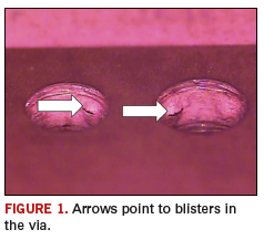
The common complaint one hears is, “The copper plating is peeling.” Ok, but where is it peeling from, off of the copper surface or from within the via? What about the interconnect? Is the peeling layer the electroless copper deposit or the electrolytic copper? These are the questions one must answer in order to properly trouble shoot the defect. FIGURE 1 shows a real-life example of a blistered or peeling deposit. The copper deposit has actually flaked off or blistered from the hole. In some cases, the deposit does not completely flake off the surface, but instead, pulls away from the hole wall. This condition is referred to as hole-wall pullaway (HWPA).Now the question is where is the origin of the blister? In this case, the good news is that we are only looking at the electroless copper. There has yet to be an electrolytic copper deposit applied to the circuit board, but that is all one can tell at this point.

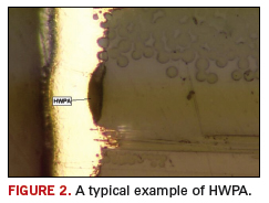
A more typical example of HWPA is depicted in FIGURE 2. The deposit pulled away from the hole-wall but did not fracture or flake off. Nonetheless, this is a defect and must be remedied. The root cause of HWPA is very similar to those that lead to flaking and blistering.
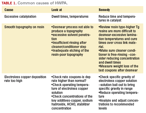
So, one is dealing with the origin of the blister or peeling deposit prior to electrolytic copper plating. TABLE 1 lists the most common causes for this type of defect. Further information about the hole wall condition can be determined by a careful review of the microsection or through SEM analysis.


Keep in mind that there is no substitute for process control. All of the operators should have a basic understanding of why certain processes must be controlled within the stated limits. This will go a long way in preventing costly rejects. PCD&F
Michael Carano is global manager for strategic business development at OM Group, Inc. and can be reached at This email address is being protected from spambots. You need JavaScript enabled to view it..


