PCB Fabrication Suppliers’ Spotlight
Published: 03 June 2009
by Kathy Nargi-Toth

Throughout the PCB supply chain, companies continue to invest in R&D to meet the changing market requirements.
We continue with the PCD&F series covering the product development teams behind the 2009NPI Award winning products.
NPI Award Winner, Dow Electronic Materials
Category: Imaging MaterialsProduct: LithoJet UV Mask
PCD&F: How did the idea for the product come about?
Dow Electronic Materials: The NA PCB manufacturers have been evolving, and today, many of them have adopted a prototyping/quick-turn business model which requires the ability to fabricate a large number of small batches of PCBs faster and more cost effectively. Lithojet products, including the UV Mask ink, were developed based on fulfilling these needs to help customers improve turn-around, yields and cost.
PCD&F: Who are the key researchers involved in the product’s research and development effort?
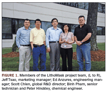
Dow Electronic Materials: The team (some of whom can be seen in FIGURE 1) on this project is quite diverse. Tom Sutter, R&D Director for Interconnect Technologies, Dow Electronic Materials, took the lead on the development team. He has been with the company for over thirteen years. Prior to joining Dow, he was a technical manager and distinguished member of the technical staff at AT&T’s printed circuit board manufacturing facility in Richmond, Virginia, so he has experience in the PCB manufacturing environment. Mr. Sutter holds a Master of Science degree in Imaging Science from the Rochester Institute of Technology in Rochester, New York.

He has been involved with imaging processes for circuit boards and other electronics applications for over 25 years.
Other team members include Kevin Cheetham, a manager and distinguished scientist for Interconnect Technologies, Dow Electronic Materials. Mr. Cheetham has 40 years experience, 20 years at Ciba and 20 years at Shipley/ Rohm and Hass Electronic Materials, in the PCB, semiconductors and related industries and was also a recipient of Hass Award in 2002.
Jeff Tsao is the marketing manager for the Interconnect Technologies, Dow Electronic Materials in Marlborough, MA. Prior to joining Dow, he was a senior system designer and product-marketing manager at Intel.
Brian Amos is the process engineering manager for Interconnect Technologies, Dow Electronic Materials in Marlborough, MA. Mr. Amos has over 23 years of industry experience, nine years in board manufacturing and 14 years with Dow on a global basis.
Dr. Scott Chien is the global R&D director for Interconnect Technologies, Dow Electronic Materials. Dr. Chien is responsible global R&D for Interconnect Technologies - Core Business including managing four R&D sites in USA, Europe, Japan and China.
Other key contributors include: Bob Barr, distinguished scientist; Ed Anzures, engineering manager; Peter Hinkley, chemical engineer and Binh Pham, senior technician.
PCD&F: Why is this product important to the PCB industry?
Dow Electronic Materials: Many OEMs do not like to switch solder mask products because it requires a requalification. Lithojet UV Mask, part of a digital imaging process, addresses improved registration and image resolution in the solder mask process, while being completely compatible with existing solder mask and developer chemistries. The solder mask doesn’t need to be changed to achieve improved registration and resolution. In addition, compared to a standard solder mask imaging process, the Lithojet UV Mask is a greener process reducing overall chemical wastes and treatment cost.
PCD&F: Can you list the product’s key benefits.
Dow Electronic Materials: The Lithojet UV Mask is compatible with existing liquid or dry film solder masks. It uses direct CAD to print methodology that eliminates the need to make or use a photo tool. The inkjet process includes real time scaling for image compensation and, as a result, the user can expect higher yield and improved consistency. In a quick-turn, high part-number environment, cycle-time is significantly reduced. The process can reduce scrap and lower material and labor usage.
NPI Award Winner, Dupont Electronic Technologies
Category: Specialty MaterialsProduct: Pyralux APR
PCD&F: How did the idea for the product come about?
DuPont: The Pyralux APR embedded resistor laminate was developed as a result of research, customer interaction and IPC committee involvement. DuPont Electronic Technologies has had an active embedded passives group for more than 10 years that has resulted in commercial and patented products, including screen printed and copper-clad embedded resistors and capacitors. Sidney Cox, DuPont Technical Research, and Rocky Hilburn, Ticer Technologies, started the initial collaboration that ultimately combined Pyralux all-polyimide laminates and Ticer TCR embedded resistor laminate. Customers in the high-reliability markets, like military and aerospace, have been looking for additional functionality in their advanced circuit products. Demand for Pyralux APR has been significantly stronger than anticipated.
PCD&F: Who are the key researchers involved in the product’s research and development effort?
DuPont: Sidney Cox, technical research, DuPont High Performance Laminates, was the primary product researcher. Gerry Sinks, senior research technician, DuPont High Performance Laminates, provided product research support. Rocky Hilburn, former technical marketing manager, Ticer Technologies, who is now with LCOA, provided product development support and advice. Scott Simpson, marketing manager, DuPont Embedded Passives, was the primary customer liaison and provided marketing direction. Tom Lantzer, manager, DuPont High Performance Laminates, was the product concept advisor.
PCD&F: Please provide some information about the customers who are adopting the process.
DuPont: The Pyralux APR embedded resistor laminate was fully commercialized in 2009. There are approximately 20 customers currently utilizing the product. Applications include on-board missile control, military land vehicles, aerospace vehicles, compact commercial handheld devices, microwave devices and other items requiring high reliability in size or weight limited applications.
PCD&F: Why is this product important to the PCB industry?
DuPont: The Pyralux APR embedded resistor laminate enables the continual drive for advanced functionality in compact electronic formats by allowing embedded resistors as part of a flexible, rigid flex or multi-layer laminate. Area and volume consumed by SMT resistors are greatly reduced by resistor inclusion in the traces and inner layer circuitry. Embedded resistor formation is easily achieved, since laminate processing is essentially the same as normal circuit processing. Device reliability is enhanced, since there are fewer solder joints, particularly beneficial for lead-free solder issues in high-performance applications.
NPI Award Winner, Enthone
Category: Final FinishProduct: OrmeSTAR Ultra
PCD&F: How did the idea for the product come about?
Enthone: The research goal was to develop a nanofinish based on an organic nanometal. The research was first initiated in 1995 under the direction of Dr. Bernhard Wessling of Ormecon GmbH. Ormecon was acquired by Enthone Inc. in September 2008. Dr. Wessling and his team saw a need in the market for a pure nanofinish. Over the next 12 years, advancements were made until finally in 2008, the nanofinish was born. The nanofinish is largely based on the organic metal predip used in the ORMECON CSN Classic immersion tin process.
PCD&F: Who are the key researchers involved in the product’s research and development effort?
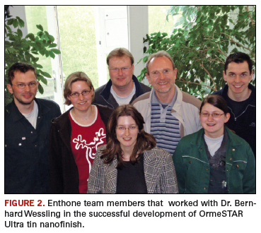
Enthone: This project has had many contributors (FIGURE 2). Dr. Bernhard Wessling was the inventor of the organic metal and the nanofinish process. During the initial phase, when the nanofinish process was found, the key engineer working on the project was Marco Thun, development engineer at Ormecon.

During the final process development, beta phase and optimization, the process was named OrmeSTAR Ultra. Many people contributed, including: Holger Merkle, manager, technical customer service; Dr. Joerg Posdorfer, research chemist, electrochemical laboratory; Susanne Blaettner, lab technician; Annett Weiman, lab technician and Dr. Melanie Rischka, manager PWB laboratories.
PCD&F: Can you provide some information about the customers and OEMs who are evaluating and qualifying the process?
Enthone: Releases of OrmeSTAR Ultra include; Sartorius AG (supplied with PWBs by fabricator manufacturer ggp Peters, Germany) and Kontron AG. The circuit boards for the qualification to Satorius AG were produced by ggp-Schaltungen. According to Andreas Töpperwien, plant director for ggp-Schaltungen, “The samples supplied for inspection to a variety of ggp customers have created a very positive response.”
PCD&F: What are the key benefits of this new final finish?
Enthone: OrmeSTAR Ultra provides a halogen-free coating that enables superior lead-free soldering with a surface conductivity comparable to pure gold. Signal transmission outperforms that of ENIG finishes. The nanofinish generates a visible coating that allows for ease of inspection and high first-pass yields with no false failures at in-circuit test. Because there are no intermediate metals present, the solder bonds directly to copper to form the industry’s strongest solder joints.
OrmeSTAR Ultra bonds with copper without a displacement reaction, ensuring long bath life, no microvoids and no solder mask interface attack. The durable coating allows for wipe downs on misprinted assemblies with no copper oxidation. Hold (dwell) time between thermal cycles is similar to other metal finishes. Application during PCB fabrication can occur before electrical test. Low application temperatures, minimal water usage and long bath life make OrmeSTAR Ultra the most environmentally friendly HASL alternative. PCD&F
Kathy Nargi-Toth is editor for Printed Circuit Design and Fab; This email address is being protected from spambots. You need JavaScript enabled to view it..


