RCC Capacitive Layers for SBU Applications
Published: 06 May 2009
by Administrator
Thin-film polymer nanocomposite capacitors can achieve high-capacitance density over large areas, reduce process steps and result in a thinner interconnect substrate.
by Rabindra N. Das, Steven G. Rosser, Konstantinos I. Papathomas, Mark D. Poliks, John M. Lauffer and Voya R. MarkovichEmbedded capacitors provide the greatest potential benefit for high-density, high-speed and low-voltage IC packages. Capacitors can be embedded into the interconnect substrate (PCB, flex, SiP, interposer) to provide decoupling, bypass, termination and frequency-determining functions.1 In order for embedded capacitors to be useful, the capacitive densities must be high enough to make layout areas reasonable. Available commercial polymer composite technology is not adequate for high-capacitance density thin-film embedded passives. One of the important processing issues in thin-film polymer nanocomposite-based capacitors is to achieve high-capacitance density on a large coating surface.
Ferroelectric-epoxy-based polymer nanocomposites have the potential to surpass conventional composites and produce thin-film capacitors over large surface areas, with high-capacitance density and low loss. Specifically, a novel flake-free and easy-to-handle resin-coated copper capacitive (RC3) nanocomposite that is capable of providing bulk-decoupling capacitance for a conventional power-power core, or for a three-layer voltage-ground-voltage type power core, is described. Epoxy dielectric resin has advantages for embedded passives in terms of processability, processing temperatures, low moisture absorption, high Tg and versatility. However, the processing and composition of nanocomposites is critical in order to achieve high quality, flake-free RC3 nanocomposites that are capable of being handled. The RC3 nanocomposite-based embedded capacitor offers many advantages over normal capacitor laminate:
- RC3 reduces processing steps and substrate thickness.
- Produces Voltage-ground-voltage (3P) cores, where two RC3 can be laminated on each side of a Cu core to double the overall capacitance (C= C1+C2).
- Used for sequential build up (SBU) technology.
- Capacitance can be changed using different bottom electrode thicknesses.
- Provides tailorable capacitance values from composition and thickness tuning.
- The capacitive composition can be provided in multiple carrier metal or organic films.
- RC3 films can be used as stand alone articles.
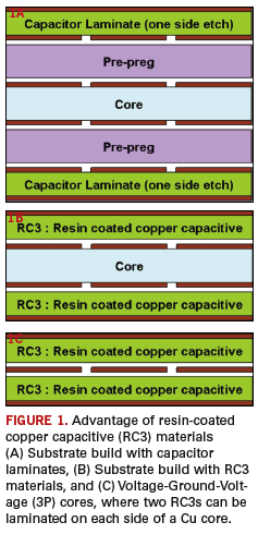
FIGURE 1 shows a schematic representation of RC3 lamination, illustrating that an RC3 capacitance layer deposited on a substrate can reduce processing steps, as well as package thickness. In the present composite, BaTiO3, or other high dielectric constant nano particles or micro particles, increases the overall dielectric constant, whereas the polymer matrix provides better processability and mechanical robustness. The effects of particle size, thickness and loading parameters on the observed electrical performance of the embedded capacitors are presented. Uniform mixing of nanoparticles in the epoxy matrix results in highly flexible and rollable thin-film (2 microns to 25 microns) RC3 capacitors. The work was extended to the development of an RC3-based multilayer embedded capacitor construction for a flip-chip plastic ball grid array package with a 300 µm core via pitch.
Results and Discussion
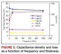
A real challenge in the development of large-area, thin-film nanocomposites is the incompatibility that exists between the typically hydrophilic nanoparticles and hydrophobic polymer matrix, which leads to nanoparticle agglomeration. As a result, inferior coatings with poor performance are obtained. We have identified a proper surface treatment that results in excellent dispersability of the nanoparticles and good quality, monolithic coatings. Appropriate surface treatment of ceramics depends on the specific processing routes. For example, Ramesh et al2 reported silane treatment of hydro thermally-prepared BaTiO3 nanoparticles. The finer details of the particles and their surface morphologies were investigated using SEM. Although the particles were highly agglomerated, with proper processing, the particles formed uniform agglomerate-free dispersions in the epoxy matrix. In case of nanocomposites, the particles in the epoxy matrix are so intimately compacted that analysis of individual particles is difficult. However, closer observation of the micrographs revealed a uniform distribution of closely packed, well-connected nanoparticles. Mixing nano-micro particles in the composites leads to noticeable surface morphology changes. Although no individual particles/grains are visible, the presence of excess epoxy may be responsible for the resulting microstructure.The electrical properties of ~8 mm2 to 20 mm2 capacitors fabricated from nanocomposite thin-films showed high-capacitance density ranging from 7 nF/in2 to 200 nF/in2, depending on composition, particle size and thickness of the coatings. FIGURE 2 shows the room temperature capacitance profile measured at 10.0 kHz to 1 MHz for an epoxy nano-micro composite thin-film as a typical representative example. It was found that with increasing frequency (10 kHz to1000 kHz), the capacitance density decreased. A capacitance density of 2.5-micron thin-films has shown high-capacitance values of 70 nF (1 MHz), which is almost four times that of 10-micron thick capacitors. Larger, effective capacitance values are expected for 2.5-micron thin-film; however, the dielectric loss increased slightly for the thin-film compared to the thick film. All of the loss values were in a narrow range of 0.014 to 0.019 at 10 kHz to 0.02 to 0.023 at 1000 kHz. Capacitance density of ferroelectric-epoxy polymer nanocomposites modified with nanomaterial (doped) was also investigated. The final film was assumed to have nanomaterials incorporated homogeneously into a ferroelectric-epoxy matrix. Capacitance density of nanomaterial modified 10-micron films was over 500 nF / in2. Capacitance of barium titanate epoxy nanocomposite, modified with nanomaterial, increases with increasing nanomaterial content. Thin-film capacitors, fabricated from barium titanate epoxy nanocomposite and modified with ~25% nanomaterial, showed capacitance density in the range of 80 nF/in2 at 1 MHz. Capacitance density of ~33% nanomaterial has shown high-capacitance value of 515 nF, which is more than six times greater than ~25% nanomaterial capacitors.
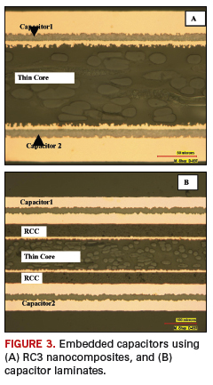
BaTiO3 epoxy nanocomposites were used to fabricate thin-film embedded capacitors, and high temperature/pressure lamination was used to embed capacitors in multilayer PCBs. The capacitor fabrication is based on a sequential build-up technology employing a first etched Cu electrode. After patterning of the electrode, the RC3 nanocomposite can be deposited and laminated within the PCB. Figure 3A shows embedded capacitors fabricated from a silica-filled epoxy/aramid paper–base substrate. The fabricated embedded capacitor can also act as a sub-composite and can be laminated with other sub-composites, making a high layer count board with embedded capacitors. Alternatively, BaTiO3 epoxy capacitor laminates can be used for embedded capacitors. Capacitor laminate can be attached to the base substrate using a prepreg, which adds extra process steps, materials and thickness to the build-up process. Figure 3B shows a representative cross section view of capacitor laminates connected to the thin core.
Test Vehicle with Multilayer Embedded Capacitors
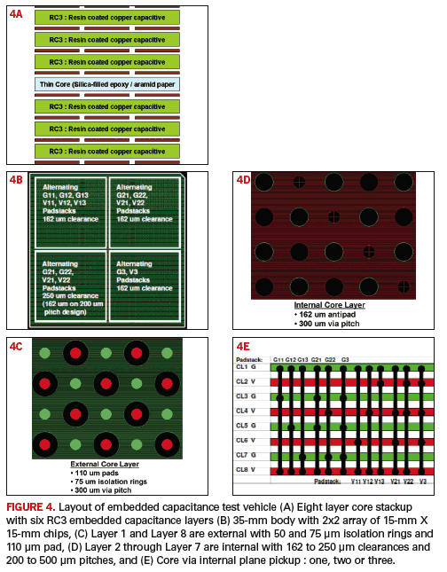
To evaluate the process, RC3 nanocomposites were used to fabricate multilayer embedded capacitance in the core of a thin-core, build-up package substrate.3-4 This particular package technology lends itself well to single-chip and SiP applications, especially in situations where space constraints are critical and miniaturization is a requirement. The capability for embedded capacitance and the associated ability to reduce discrete component counts create significant additional miniaturization leverage.This multilayer structure starts with a core that is constructed using a 110-µm thick dielectric layer composed of silica-filled epoxy with aramid paper fibers sandwiched between Cu layers. The optimized ferroelectric polymer-based RC3 nanocomposites were used to build up thin-film multilayer (layers 4,6,8) cores with embedded capacitance, and high temperature/pressure lamination was used to embed capacitance in the multilayer construction. The capacitor fabrication is based on a sequential build-up technology employing a first patternable electrode. After patterning of the electrode, the RC3 nanocomposite can be laminated within the structure. Capacitance values are defined by the feature size, thickness and dielectric constant of the polymer-ceramic compositions.
A test vehicle (TV) was designed with various sizes, thickness and values of embedded capacitors. Individual 35-mm substrates with a two-by-two array of 15 mm² isolated epoxy-based regions were designed, each having six RC3-based embedded capacitance layers. The total TV core consisted of eight metal layers. Design features, including antipad diameters, internal plane pickups for vias and core via pitch, were varied within each 15 mm² region, and probe pads were added for testing capability. The design incorporated four core via pitches (200 µm, 300 µm, 400 µm, 500 µm) and three possible plane pickups that include external plus one internal, external plus two internals and external plus three internals. Antipads of 162 µm and 250 µm were used. FIGURE 4 shows embedded capacitor layouts.
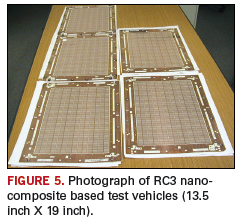
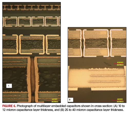
FIGURES 5 and 6 show top and cross section views of multilayer embedded capacitors. It is possible to make a wide variety of capacitance layers with different thicknesses. Desired thickness of the film can be achieved by controlling the viscosity of the coatings, composition and the number of layers deposited. In the present process, we can easily laminate thin-films from about 8 microns to about 50 microns. Figure 6 illustrates a variety of multilayer embedded capacitors, where capacitors were sequentially applied on the surface. This allows multiple capacitor layers in a thin total structure. The resin-coated copper capacitive nanocomposite layer does not need to supply any structural support, it can be very thin and achieve high values of capacitance per unit area. Also, since it is not structural, the material choices expand significantly.
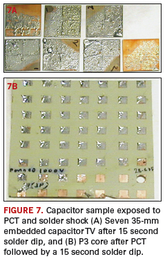
Although embedded capacitors are more reliable by eliminating solder joints, they also introduce other potential defects such as cracks, material mismatch and delamination. Embedded capacitors are of little value unless they can survive the same rigors of testing that modules or boards would receive. Package and sub-composite level reliability of multilayer embedded capacitors in the test vehicle were further examined by IR-reflow (3X, 225ËšC), pressure cooker test (PCT) and solder shock. In PCT, samples were exposed to 100% humidity, with a constant pressure 19 psi at 121ËšC. No intrinsic failure mechanisms were observed, and there was no cracking or delamination in the materials. Barium titanate epoxy nanocomposite capacitors were also exposed to PCT (2 hrs) followed by a 15-second solder dip at 260o C. There was no delamination observed after PCT and solder shock. In general, solder dip/shock will accentuate PCT induced defects and cause delamination. FIGURE 7 shows multilayer capacitor samples after exposure to PCT and solder shock.
Conclusion
Nanotechnology is able to produce high-capacitance density (7 nF/inch2 to 500 nF/inch2), large area, thin-film capacitors with controlled thickness from about 2 microns to about 50 microns for a series of epoxy-based nano micro composites. SEM micrographs showed uniform particle distribution in the composites, while lamination was used to fabricate embedded test capacitors in a multilayer PCB. Embedded test capacitors were stable after 3x IR-reflow, PCT and solder shock. This is an integrated approach centering on three interrelated fronts: the material’s development and characterization; fabrication; and design and electrical characterization at the substrate level. The overall approach lends itself to package miniaturization because capacitance can be increased through multiple layers and reduced thickness to give the desired values in a smaller area. PCD&FAcknowledgments
The authors acknowledge the valuable contributions of B. Mackerthy, R. Japp, T. Antesberger, S. Hurban, C. Carver, M. Shay and G. Kohut.References
1. “Passive Integration: Easier Said Than Done,” Prismark Partners LLC, August 1997.2. Ramesh S., Shutzberg B. A., Haung C., Gao J., Giannelis E. P., “Dielectric nanocomposites for integral thin-film capacitors: Materials design, fabrication, and integration issues,” IEEE Transactions on Advanced Packaging, Vol. 26, No. 1, (2003), pp. 17-24.
3. Jadhav, V., Moore S., Palomaki, C., and Tran, S., “Flip Chip Assembly Challenges Using High Density, Thin Core Carriers,” Proc 55th Electronic Components and Technology Conf, May 2005, pp.314-319.
4. Memis, I. “Wireability Comparison of Flip Chip Substrates as a Function of Chip Design and Substrate Capability,” International Conference and Exhibition on Device Packaging, Scottsdale, AZ, 2005.
Rabindra Das is a senior advisory technologist; This email address is being protected from spambots. You need JavaScript enabled to view it.; Steven Rosser is an electrical applications engineer; This email address is being protected from spambots. You need JavaScript enabled to view it. Konstantinos I. Papathomas is a senior advisory technologist; This email address is being protected from spambots. You need JavaScript enabled to view it.; Mark Poliks is R&D director, university relationships & consortiums; This email address is being protected from spambots. You need JavaScript enabled to view it.; John Lauffer is a senior advisory technologist; This email address is being protected from spambots. You need JavaScript enabled to view it. and Voya Markovich is senior VP R&D and CTO; This email address is being protected from spambots. You need JavaScript enabled to view it., all working for Endicott Interconnect.


