Short Circuiting OSP / ENIG Galvanic Etch
Published: 05 May 2009
by Jim B. Kenny

An alternative approach to the etching process promises to open up the design window for mixed-metal finishes.
As circuit board designers, fabricators and assemblers work together to provide the most robust products, one final finish option that is very common, especially among handset designers, is electroless nickel/immersion gold (ENIG), used in conjunction with OSP. This particular finish combination enables a circuit board to have excellent grounding and key contact pad performance with ENIG and also yields the highest, most consistent solder joint strength possible with solder-to-copper bonds on bare copper surface mount pads coated with OSP. Many handheld devices, available on the market today, incorporate this mixed surface finish technology, due to its excellent solder joint strength as demonstrated by drop test performance.However, there are several issues that need to be addressed with this combination of surface finishes. One issue that can arise from this type of construction is a galvanic etch effect at the copper nickel-gold interface. If a large nickel-gold feature is attached to a copper trace or pad, the electrochemical potential from the nickel-gold is transferred to the exposed copper, creating an extremely active localized etch. This localized hyperactive etch can result in pad size reduction or trace width reduction until an opening is created or the pad size is reduced below what can be soldered.
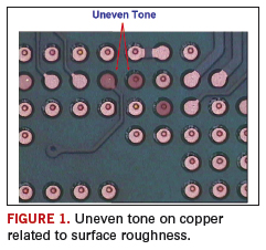
The second issue that can arise, an uneven tone problem, also finds its origins with a galvanic effect. When circuits are processed with certain grounding configurations, some copper pads will appear dark, while others will appear bright. This light and dark effect repeats itself from image to image on the same features. An example of the issue is shown in FIGURE 1.

The reason the copper appears to be two different colors is due to differences in the roughness of the surface topography. The darker pads are rougher, on average, than the brighter pads. This increased topography relief reduces reflectivity, making the pads appear dark. This is an etching issue and is not an indicator of an organic solderability preservative problem.
New technology available in the marketplace eliminates these types of problems. New etches with different acid packages are not only compatible with mixed-metal finishes, but also more stable, produce more uniform etch color on high and low current density areas of the circuit board and provide a mild anti-tarnish capability to improve process flexibility.
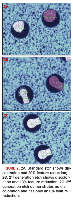
Recently, tests were run with a specific part a customer was having processing issues with. Standard etches resulted in too great a feature reduction and an uneven tone. The second-generation etch was able to help with the feature size reduction but not the uneven tone. The third-generation etch resolved both issues. (FIGURE 2A, 2B and 2C)

New etch technology promises to open up the design window for mixed-metal finishes. The ability to etch sufficient amounts to provide a good solderable surface no longer needs to be compromised by localized high etch rates. The new technology provides a more uniform etch depth, appearance and color on all copper features. Bath stability and consistency remain intact over greater periods of time, allowing for fewer issues and a wider process window. PCD&F
Acknowledgements
Zheng Bo, Enthone ATC Group, Singapore.Jim Kenny is global product line manager, PWB final finishes, Enthone, Inc; This email address is being protected from spambots. You need JavaScript enabled to view it..


