Effective Decoupling Capacitors
Published: 05 May 2009
by Dr. Bruce Archambeault

Mount capacitors on the bottom side of the PCB to reduce connection inductance when paired planes are deep in the stack up.
Decoupling capacitors serve two purposes: to provide charge to the ICs for functionality and to maintain low impedance between power and ground-reference planes in order to reduce/eliminate plane resonances, which would increase EMI emissions.The effectiveness of the various grid densities of distributed decoupling capacitors has been debated for years. On one hand, it is understood that more densely distributed decoupling capacitors will provide the best EMC performance (low impedance across the plane pairs), but, when more capacitors are used, the PCB real estate, as well as the cost of the total number of capacitors, increases.
A study was conducted to help define the effectiveness for various proposed decoupling capacitor grid densities. Since the connection inductance will have a major impact on the effectiveness of the capacitors, a variety of connection inductance values were included in the study.
Configuration
A board size of 10 inch by 12 inch was used for this study. The board size will determine the actual resonant frequencies, but the overall effects will be consistent for any board size. The dielectric thickness was set to 5 mils and 10 mils, in order to include typical boards.Grid densities of 1000 mils by 1000 mils, 1250 mils by 1250 mils, 1500 mils by 1500 mils and 2000 mils by 2000 mils were simulated using EZ-PowerPlane1, and connection inductance of 0.5 nH, 1.0 nH, 2.0 nH, 3.0 nH and 4.0 nH were included. For purposes of this study, the connection inductance includes the capacitor’s equivalent series inductance (ESL). Depending on the size of the surface mount capacitor, typical values for ESL range from 0.2 nH to 0.5 nH. However, this is not the complete story on the inductance associated with decoupling capacitors!
Connection Inductance
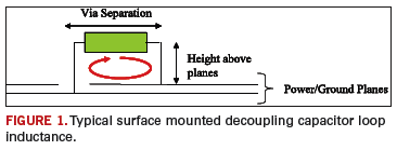
The connection inductance depends on the distance between the vias, which connect the capacitor to the planes, and the distance from the top (or bottom) mounting location to the planes that are to be decoupled.2 FIGURE 1 shows a side view of the typical capacitor mounting on a PCB, and TABLE 1 shows some calculated3 connection inductances (without ESL) for 0805-, 0603- and 0402-sized SMT capacitors.2-3
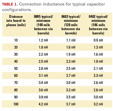
These values are calculated with the example of 7 mils to 8 mils from capacitor to mounting pad edge, 20 mils from capacitor mounting pad edge to via pad, via pad diameter of 20 mils, via barrel size of 10 mils and trace width equal to 20 mils. The absolute minimum distance from the via pad to the capacitor mounting pad edge is reported to be 10 mils, but typically 20 mils is used to be safe.
Results
The results in FIGURES 2 to 3 show the impedance between the planes for both 5-mil and 10-mil spacing between the planes. The inductance includes both the connection inductance and the capacitor's specified ESL.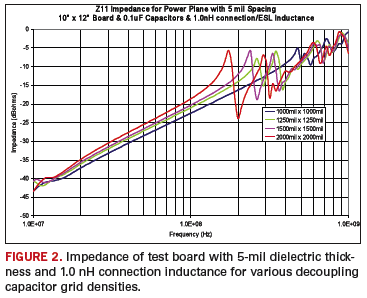
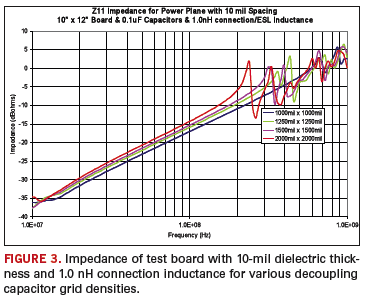
TABLE 2 shows the first resonant frequency for 5 mil spacing between the planes, and TABLE 3 shows the frequency, where the impedance rises above 0.1 ohms (-20 dBohms). TABLE 4 shows the first resonant frequency for 10-mil spacing between the planes, and TABLE 5 shows the frequency, where the impedance rises above 0.1 ohms (-20 dBohms). Since the primary method to avoid resonances is to maintain a low impedance, 0.1 ohms is chosen as a low impedance target. The actual target impedance may vary depending on the specific product.
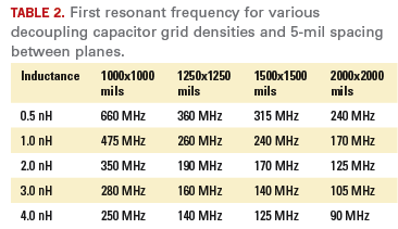
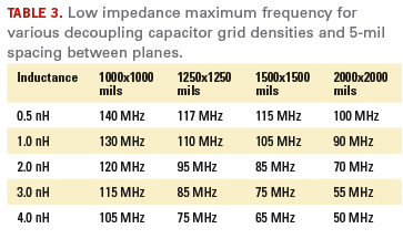
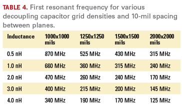
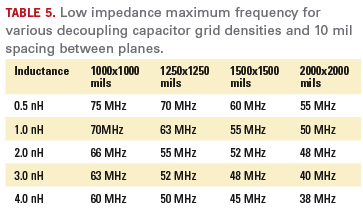
Table 1 should be used together with Table 2 to Table 5 to find the frequency where a grid density is no longer effective.
For example, in the case of a PCB stack up using 5-mil spacing between the planes and a pair of planes that are 10 mils from the top of the PCB, when 0603-sizes capacitors are used, the expected connection inductance is 1.1 nH. When a typical ESL of 0.5 nH is added, we have total inductance of 1.6 nH. The expected first resonant frequency would be about 400 MHz for a 1000 mil by 1000 mil grid and about 200 MHz for a 1500 mil by1500 mil grid.
However, if the same pair of planes are deeper into the PCB stack up and the distance to the planes becomes 50 mils, the expected connection inductance becomes 2.5 nH. When ESL is added, the total inductance for the capacitor is 3.0 nH. The expected first resonant frequency would be about 115 MHz for a 1000 mil by1000 mil grid and about 75 MHz for a 1500 mil by1500 mil grid.
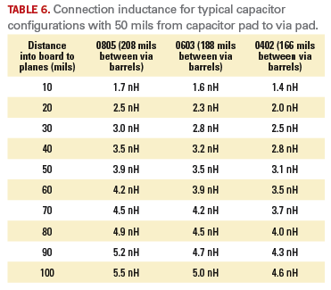
If the distance between the via pad edge and the capacitor pad edge is increased to 50 mils on each side, the resulting inductance values are shown in TABLE 6. With the exception of plane pairs close to the surface, the inductance can be seen to increase by more than 1 nH over the similar cases in Table 1. Once the value of inductance is determined, the effective range of the decoupling capacitor grid density is seen in Table 2 through Table 5.
Conclusion
It can be seen that the effect of connection inductance (and ESL) limits the effectiveness of decoupling capacitors, especially when the grid density is relaxed to larger spacing. If the design goal is to have no resonances below 100 MHz to 200 MHz, then a smaller grid density must be used. Even then, depending on the depth of the plane pair in the PCB stackup, the grid density may not be effective.The depth of the plane pair in the PCB stackup indicates when the decoupling capacitors should be mounted on the top of the PCB and when it is more effective to mount them on the bottom. When the pair of planes is deep in the PCB stack up, there will be less connection inductance when the capacitors are mounted on the bottom side of the PCB. PCD&F
References
1. www.ems-plus.com2. Knighten, James L., Bruce Archambeault, Jun Fan, Samuel Connor, James L. Drewniak, “PDN Design Strategies: II. Ceramic SMT Decoupling Capacitors – Does Location Matter?” IEEE EMC Society Newsletter, Winter 2006, pp. 56-67.
3. Fan, Jun, Wei Cui, James L. Drewniak, Thomas Van Doren and James L. Knighten, “Estimating the Noise Mitigating Effect of Local Decoupling in Printed Circuit Boards,” IEEE Trans. on Advanced Packaging, Vol. 25, No. 2, May 2002, pp. 154-165.
Dr. Bruce Archambeault is an IBM distinguished engineer at IBM in Research Triangle Park, NC. He can be contacted at This email address is being protected from spambots. You need JavaScript enabled to view it..


