Concurrent RF/Microwave PCB Design

When RF and PCB design teams co-design as equals, the design can meet performance goals in less time.
by Dr. Michael C. Heimlich and Per Viklund
Designing RF (including microwave) circuits concurrently with digital and analog, and transferring these circuits to a manufacturable, DRC-correct PCB has previously been impeded by the very productivity tools used for their respective domains. File-based translation, that came to the forefront with IFF translation in the mid-1990s, has never lived up to its promised productivity gain and cycle-time reduction. A flow achieving concurrency between RF/microwave design, EM analysis and circuit simulation, along with PCB library management, digital/AMS implementation and manufacturing verification and preparation, has recently been demonstrated.
A survey of design styles, techniques and/or processes would normally show that it is rare for previously disparate design flows to merge. If new capabilities come along, like design for manufacturing (DFM) or signal integrity analysis, they are normally added to the existing flow (shoehorned in) so that design cycle times improve either by incrementally removing time from a single pass or by taking board respins out of the design process as a whole. Sometimes, flows collide, and there is often an uneasy co-existence at best where data gets passed “over the transom,” and the necessary task of decoding what has been sent adds far too much time to the design cycle.
While the wireless phenomenon has marched on in the past decade, PCB and RF have undergone a quiet revolution. By successfully merging two long-standing, independent and successful flows, the ability to co-design the RF electrical performance, while preparing a full-up PCB for manufacturing, has emerged.
A Model for Convergence of PCB and RF
RF and PCB have been cohabitating for years, as both RF layer and component count have increased and PCB frequency or clock-rate has likewise been increasing. Not so long ago, an RF design was a single-layer affair on exotic material (i.e. alumina) with a handful of components. The digital data rate on a traditional multilayer PCB may have been in the tens, or barely hundreds, of megahertz. Neither design environment had much use or knowledge of the other.
But things have changed dramatically in the last decade. Now, digital data rates on PCBs are well into the gigahertz range, with processor clock speeds of a few gigahertz and serial data rates regularly at 10 GHz and up to 20 GHz. The electrons don’t care that they are no longer on alumina, and they don’t care that PCB designers call the board or block “digital” or “analog”; a signal at a GHz is an RF/microwave signal. RF power amplifier and front-end modules for mobile handsets previously may have been a chip in a package, now they are six to eight layer “modules” with dozens of components squeezed into a form factor the size of a thumbnail. The module may not be a 24-layer, 1-meter-square panel, but it sure isn’t a couple of surface mount devices (SMDs) on alumina.
Shortcomings of Previous Flows
Early attempts to merge these flows were done prior to the design community seeing this as the current state-of-the-art, perhaps for a few visionaries or madmen. The IFF file format was popularized in the mid-1990s and was the centerpiece of several integration efforts spearheaded by DARPA, EDA vendors and enlightened customers seeing the future of wireless telecommunications. While these attempts supported IFF import/export capability for nearly every PCB and RF/microwave EDA tool by the early half of this decade, the solution was found lacking for several reasons, despite the fact that IFF is a very capable ASCII file format.
Perhaps the biggest drawback to IFF is the need to have duplicate libraries (master-slave approach). In practice, this comes down to taking the golden standard, the PCB library, and creating a slave library suitable for the RF/microwave flow’s simulation-centric nature. While IFF does have a “placeholder” for defining symbol, part number, footprints and padstacks, it is still incapable of taking a randomly selected part from any PCB designer’s parts library and guaranteeing that a simulatable model will appear in the RF tool upon import. Efforts to implement and to maintain IFF-based flows became heroic tasks in maintaining duplicate databases. In some cases, these were accompanied by a total redesign of library management system implementations to accommodate the explosion in RF-related attributes. Something as simple as standard pin placement for a padstack has no meaning in RF/microwave tools, since the simulation model may have been derived with the “reference” location at the front- or back-edge of the pad, but rarely in the center.
The first nail in the coffin for the file-based flows was the realization that they really supported no flow at all. The IFF files going from the RF to the PCB tool, one for the schematic and one for the layout, disabled the ability for the RF designer to directly incorporate, through EDA automation, any changes made in the PCB tool from that point on. The link to RF circuit-based simulation was broken, especially when the easiest way to get the modified copper was simply by bringing back to the RF tool a DXF file, running an EM solver on it and then somehow manually stitching back into the RF schematic a multi-pin count part that was the beautifully, handcrafted microstrip and stripline elements of the RF designers art.
And the final nail in the coffin for the IFF-based approach was the rising complexity of the RF sections. Previously, with just a handful of parts and plenty of space, it was a somewhat trivial task for the RF designer to create rudimentary artwork that met the DRC and DFM requirements. RF/microwave tools work well with a couple of layers and a dozen components, but as this grew to dozens of components and layers for several RF blocks, and with modern, aggressive trace widths and spacing, it became apparent that primetime, enterprise PCB DRC and DFM were needed to get these RF designs into manufacturing. However, the PCB designer cannot have carte blanche to move traces and components around for the sake of DRC and at the expense of electrical performance, as the board has to meet its RF electrical criteria. Moving just copper back to the RF/microwave tool is time-consuming and disconnected from the real circuit-level simulation that needs to be done at signoff. Trying to get 0201 SMDs placed for DRC is nearly impossible in an RF/microwave tool.
Flow Solution
The more viable solution to concurrent RF/microwave and PCB design is to start from the ground up, with an open mind and a fresh approach — one that treats each design team as equal partners. Based on the key problems identified, it was clear that a file-based ASCII translation was not going to work simply because this was not a flow but a simplistic means to an ill-conceived end. Designers needed true automation, where the databases were actually created and/or updated as data flowed back and forth. Besides the obvious bidirectional flow of schematic and layout data, where changes in either datum are instantly updated in the other, this data flow had to be on demand at all appropriate times in the flow.
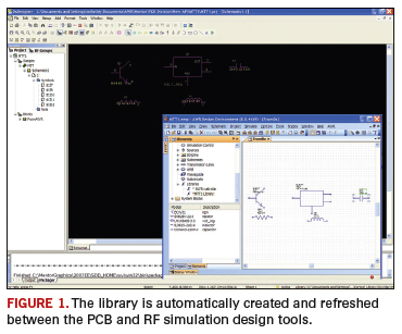
First and foremost, the library is created automatically in the RF/microwave tool based on the “golden” PCB library as seen in FIGURE 1. RF model generation defaults to passives based on the symbol name, and more complex parts can either use a single attribute to specify the model or can create a placeholder model in hierarchy in the RF tool, since more than a few RF engineers create a new model for each design based on the stackup and manufacturing rules. Footprints can use the default “center” pin placement in the RF/microwave tool’s layout or a single attribute can be used to specify moving the pin location to the front or back edge of the pad. Automation in the integration uses the component body to determine “front” and “back” and move the pin dynamically for each padstack instance. The library is created with the first connection of the PCB tool to the RF tool and is updated, in case of library changes, with each subsequent connection. The library is, therefore, always automatically generated and refreshed and never gets stale.

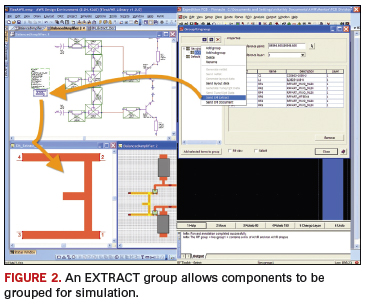
Secondly, RF circuit simulation is the central piece of the flow, regardless of work on the schematic or layout. When the schematic is sent from the PCB side to the RF side, the microstrip and stripline substrate definitions, because of their relation to the stackup, are sent along to ensure proper circuit level simulation of the copper. Parameter-based shape generators for these parts, a standard aspect of RF tools for several decades, are part of the layout flow and allow the RF blocks in the schematic to be placed and “routed” in the layout. Changes to the blocks can be shipped off to the RF layout tool, but because of the unified data model on the RF side—a single database from which both the schematic and layout are drawn—any parametric schematic change is immediately rendered in the RF layout view, thus, allowing immediate layout-based circuit simulation. This is further enhanced by allowing the PCB layout tool the ability to create EXTRACT groups, illustrated in FIGURE 2, where an EXTRACT group is nothing more than identifying components which should be collected together for EM analysis, with the catch that the RF schematic controls the EM analysis so that there is no need to stitch back in the resulting, high pin-count S-parameter file for EM simulation.

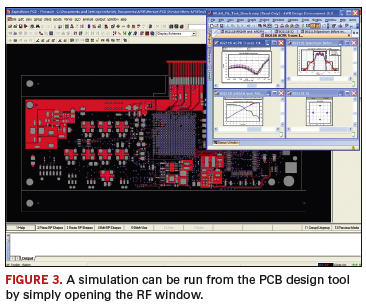
The result is a true co-design flow where the RF designers have full access to the PCB data that they need to do top-down, parametric circuit design, and the PCB design has no RF simulation limitations, as the total design is assembled and prepared for manufacturing. There are no more bottlenecks, while trying to make the board manufacturable without losing RF/microwave simulation signoff. As the project gets down to crunch time, the PCB designer can be making changes in the RF block and, with a couple of mouse clicks, send the entire, circuit-level simulatable block to the RF engineer for simulation and recertification. It can also be done right from the PCB tool by viewing a window from the RF tool, as seen in FIGURE 3. Changes made interactively for DRC component placement in the PCB tool introduce no cycle-time penalty in data transfer for resimulating the copper with an EXTRACT’ed EM solve or globally at the RF circuit level.

Design Equality Means Design Efficiency
It is a staunch reality to everyone involved in RF design that the traditional flow frequently resulted in too many design iterations, and due to the manual craftsmanship involved in every iteration of the design cycles, a long design timeframe. The end result was high design costs, long design cycles and a risk of lost market opportunities.
In an attempt to recover the stretched timeline, design teams reduced the number of simulations made, and while this could significantly shorten the cycle time (as the manual iteration work is eliminated), it dramatically increased the risk for late cycle issues and errors that could set a project back beyond rescue.
The only viable solution is to adopt a design flow that enables seamless integration between PCB and RF design so that simulations can be much more frequent without any manual patchwork. This way, the RF circuits can be implemented on the PCB, including modifications to fit in the small space designated, while still ensuring that the RF circuit meets its specs. Likewise, this enables the PCB tool to make use of the design rule checks made by the RF design tool and vice versa. In such a flow, it’s no longer a matter of making changes, hoping it will work, but validating as changes are being made in both PCB and RF environment to constantly keep the circuit within specifications both electrically and manufacturing-wise.
As a bonus, the integrated flow lends itself perfectly to concurrent design, where multiple PCB engineers and multiple RF designers can work concurrently to reach design closure in much shorter times than traditional sequential flows. In short — a perfect foundation for a single iteration RF/mixed technology design flow, with cycle times that are only a fraction of traditional methods.
Conclusion
RF and PCB have been more or less merging for years, as RF layer and component counts have increased and PCB frequency or clock-rate has been increasing. Prior master-slave mentalities to a successful concurrent flow via IFF failed to deliver the gains as promised. When a true partnering approach is considered, one in which the RF and PCB design teams are perceived and treated as equals, the design itself wins by achieving its performance goals in less time, with fewer headaches and, hopefully, much market success. PCD&F
Dr. Michael C. Heimlich is director, microwave office and AWR SI marketing at Applied Wave Research Corporation; This email address is being protected from spambots. You need JavaScript enabled to view it.. Per Viklund is director of IC packaging & RF with Mentor Graphics, Systems Design Division; This email address is being protected from spambots. You need JavaScript enabled to view it..


