Processing High Frequency Materials, Part 2
Understanding the primary and secondary performance requirements in a high frequency application can help designers determine the most suitable materials to use.
Ed. – Part 1 appeared in the March issue. Both parts are presented here.
Specialty high frequency circuit materials have been used in the PCB industry for decades. There are several attributes of these materials that are very unique when compared to the more traditional FR-4 materials. Understanding these attributes can help the OEM, designer and fabricator optimize the application and maximize the potential for improved electrical performance on the products that are being developed. There are additional, non-electrical advantages to these materials as well. In order to realize the full potential that these materials have to offer, it is important to understand the specific application and design constraints that need to be addressed.
Most high frequency applications will place multiple demands on the PCB material, and some of the requirements may be contradictory. For a specific application, one requirement is often paramount, while the others are secondary. Understanding the primary design considerations and specific requirements for the high frequency materials will allow the designer to choose the optimum material for the application. Several example applications will demonstrate how the various attributes of the product need to be considered in order to determine the optimum material to be used.
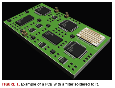
The first application example is a small filter circuit using high frequency materials that will be soldered to a larger FR-4 circuit board, as shown in FIGURE 1. The completed assembly will be housed inside a sealed enclosure and will operate in an outdoor environment that varies greatly by the seasons. Added to this is the specific heat generated by the equipment. Temperatures inside the enclosure could vary from –25 °C to +70° C.
Filter circuits typically need a material with very consistent dielectric constant (Dk). This means consistent Dk within a sheet of circuit material, as well as from lot-to-lot. This is required so the filters being attached to the FR-4 circuits will have the same performance, and minimal part-by-part tuning will be necessary. This filter will be a double-sided plated through-hole (PTH) circuit, with the ground plane on the bottom and the signal plane on the top, coupled to the FR-4 circuit board using a microstrip edge coupler. As previously mentioned, most high frequency applications have more than one demand on these circuit materials. In this case, the consistent Dk is paramount, but there are other demands that also need to be considered as secondary.
All circuit materials have some amount of growth or shrinkage due to heating or cooling of the material, due to the coefficient of thermal expansion (CTE). In this case, the CTE may not appear to be important, but it can be critical. Once the filter is soldered onto the FR-4 circuit board, the solder joints become a rigid bridge between the FR-4 circuit and the high frequency filter. When the unit experiences a change from 0° C to +30° C (as an example), the FR-4 and the filter circuit will expand. If the CTE is significantly different between the FR-4 and the filter material, stresses can develop at the solder joints that connect the circuit board to the filter, and this may become an issue over time. In most cases, one excursion from 0° C to +30° C is not a problem, but with repeated cycling, the solder joints become stressed and the electrical connection can be compromised.
Another critical issue is that of the material’s temperature coefficient of dielectric constant (TC Dk). Each type of circuit material has a property where the Dk value can change with a temperature change, and that is the temperature coefficient of dielectric constant. With certain circuit materials, the Dk may appear to be good and consistent when tested at room temperature; however, as the temperature changes, the Dk can change and cause the filter to perform significantly different than as designed.
An additional consideration is the assembly operation, where the filter is soldered to the FR-4 circuit board. Since the filter has plated through-hole vias, the z-axis (thickness) CTE can become a concern during the soldering operation. Depending on the design of the filter and the FR-4 circuit board, the dwell time during soldering may need to be adjusted, particularly if thick materials and heavy copper are used. If the circuit material has a higher z-axis CTE than the filter material, an extended dwell at elevated temperatures can cause damage to the plated through-hole vias and degrade the electrical connection from the signal plane to the ground plane.
Lastly, if the filter is intended to operate over a wide range of frequencies, it is important to understand that most circuit materials will have different Dk values at different frequencies. It should also be considered that some materials are more stable than others.
In summary for this application example, this filter circuit should use a material that has a tight tolerance for Dk, a CTE that is closely matched to FR4 in the x-y plane, a low TC Dk, a low z-axis CTE and a stable Dk vs. frequency curve. There are many high frequency circuit materials to choose from but finding the right circuit material, which fills all of these requirements, will reduce the available choices. A comparison between the properties of a standard FR-4 circuit material and the material under consideration for the best choice is highly recommended. For this example, the typical values regarding the properties of interest for a standard FR-4 material are shown in FIGURE 2. The user will need to determine the fitness for use of the selected materials by conducting appropriate short-term and long-term reliability testing as dictated by the needs of the application.

Additionally, if it were critical to reduce the physical size of the filter, a different circuit material with a higher dielectric constant may have been the right choice. A material with a higher dielectric constant will allow the circuit to be reduced in size while still performing the same function. The high frequency circuit material used for this filter application may not actually be used at a relatively high frequency. The material may have been selected due to its tight Dk values and the other properties mentioned. Another item where most high frequency materials have an advantage over more traditional FR-4 circuit materials is minimal moisture absorption. Having low moisture absorption is important for several reasons, including the fact that in high frequency applications where consistent Dk is critical, moisture absorption can be a problem. Water has a Dk value of about 70, and even a small amount of moisture absorbed into a high frequency circuit or a controlled impedance circuit can change the electrical performance.
The second application example is a microstrip circuit that will need to be formed to a specific shape around a mandrel that has a 0.5-inch diameter. The electrical concerns are primarily low insertion losses (< 0.05 dB/in), tightly controlled impedance (50 ohms +/- 5%) and operating considerations at 900 MHz. Typically, an application operating at 900 MHz is not considered high frequency and more traditional FR-4 materials could normally be used. There are however, other electrical concerns that drive material selection to a high frequency grade material in this example.
The need for tightly controlled impedance translates to a substrate that must have tightly controlled thickness and Dk values. Traditional FR-4 materials will not control these attributes nearly as well as high frequency circuit materials. Of course, the etching of the conductor width will need to be tightly controlled at the circuit fabricator to meet the controlled impedance targets.
Overall, the concern of low insertion loss can be rather complicated. There are many issues that can affect this circuit property such as: connectors, signal launch design, plating finish on the copper conductors, dissipation factor of the substrate, copper roughness, circuit geometry and some assembly processes. When choosing the material that will give the best advantage for insertion loss, a material with low dissipation factor, smooth copper and low moisture absorption would be optimum. Also, the circuit design should use a relatively thick substrate.
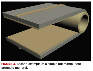
In this case, there are additional concerns with the mechanical challenge of forming a circuit around a mandrel (FIGURE 3). Typically, a thinner substrate with no glass reinforcement will be better for forming the circuit and will generate less strain on the copper layers. Also, the copper type should be rolled wrought or rolled annealed copper, which has a grain structure that is optimum for elongation in the x-y plane.1
Another consideration could be the type of plating finish applied to the copper conductors of the microstrip. If ENIG (electroless nickel / immersion gold) is used, then the nickel is brittle and can be problematic for bending. Also, the ENIG process will typically deposit a thickness of approximately 100 microinches to 200 microinches of nickel and about 5 microinches of gold. With the operating frequency at 900 MHz, the skin effects will force the signal to use about 87 microinches of conductor. That means the signal energy will predominately use the nickel layer, and nickel will cause an increase in conductor losses and ultimately insertion losses. This is due to the fact that nickel is less conductive than copper and has a permeability value that is much greater than copper. The permeability value will adversely affect the magnetic fields of the propagating waves.
For this application, designers should choose a high frequency material that has a tight control of the Dk and thickness tolerances, low dissipation factor, smooth copper, non-glass reinforcement, low moisture absorption and a non-nickel/gold finish. To determine the optimum thickness, there will need to be a trade-off between mechanical and electrical properties. For a one-time bend, there is a rule of thumb that states the strain on the copper should be approximately 2% or less. FIGURE 4 shows a comparative table of different materials and thicknesses in regards to the mechanical stress values and insertion losses.

In Figure 4, it can be seen from the first model to the second that the thickness of the substrate decreases. The decrease in thickness improved the mechanical stress significantly. A decrease in the substrate thickness will force a decrease of the conductor width in order to maintain 50 ohms. The decreased conductor width will increase the conductor loss, and ultimately, the insertion loss.
When going from the second to the third model, a different material was selected that had a lower dielectric constant and lower dissipation factor while still maintaining the same substrate thickness. The lower dielectric constant dictates an increase in conductor width to maintain 50 ohms. The increase in conductor width lowers conductor losses, and the decrease in dissipation factor lowers dielectric losses. With lower conductor and dielectric losses, insertion loss also decreases.
It can be seen that the stress number is a little higher than would be desired, but when looking at other models, this appears to be the best-case scenario. In reality, this may be good enough for the actual application. If in practice this model does not result in good, repeatable bends, the mandrel may need to be increased in size to lower the stress.
When using high frequency materials in a PCB design, it is important to understand the primary performance requirements of the final product so that the best material can be selected for use. Most high frequency materials are used in specific applications where low electrical loss and uniform electrical performance across frequencies is needed. In addition, low moisture adsorption and excellent chemical resistance are salient properties of many high frequency materials and can be advantageous in specific environmental applications.
The electrical benefits of high frequency materials are well understood. There are, however, a number of fabrication concerns related to the most commonly used high frequency materials. These materials include PTFE (Teflon), PTFE with ceramic fillers and non-PTFE thermoset resin systems with ceramic loading, as well as bonding materials used to make multilayers from these materials. In addition, a newer material, LCP (Liquid Crystalline Polymer), while not as commonly used, offers unique properties that enable evolving PCB applications and several hybrid circuit constructions. LCP also has some specific fabrication guidelines that are different
The high frequency circuit materials that have been used in the industry for the longest period of time are the PTFE materials. Most of these materials are not pure PTFE. They can have either some small amount of micro-fiber glass impregnated into the substrate or can be PTFE with woven glass reinforcement. In some cases, the PTFE is ceramic-filled. In general, and in comparison to the other types of high frequency materials, the nearly pure PTFE without woven glass can be the most challenging type of circuit material to use in PCB fabrication.
There are several reasons for this: PTFE has a high CTE; PTFE doesn’t let other materials (such as plating) adhere to it easily; and the PTFE substrate is soft and can be easily distorted. From an electrical performance perspective, the PTFE substrates that are typically the best to use are the ceramic-filled PTFE substrates because they are much easier to process through PCB fabrication.
The main PTFE PCB fabrication issues are: laminating the PTFE materials with other bonding materials; processing without scrubbing or mechanically altering the substrate; drilling without any smear; through-hole hole-wall preparation to increase adhesion of the copper plating in the PTH; dimensional stability (scaling) issues; and practices to minimize handling damage of the soft substrate.
Most bonding materials used in the PCB industry can be used as a bonding layer for a multilayer PTFE circuit, with some precautions. The main point of interest would be not to alter the exposed substrate surface. After the copper etching process, the exposed PTFE substrate surface should not be mechanically altered in any way. The mirror image of the copper profile, from the copper that was etched away, will be the surface roughness of the exposed PTFE. This surface will need to remain unaltered in order to assist with mechanical bonding to the bonding material.
A scrubbing process will actually polish the soft PTFE surface and have an adverse effect on the bonding, so it is not necessary to perform a process on the exposed PTFE substrate to activate it in order to accept a bonding material. There is a benefit to performing a bake cycle for the ceramic-filled PTFE just prior to lamination. The bake cycle is intended to drive off any possibly absorbed processing chemistry and can be done at 121°C (250°F) for 1 hour to 2 hours. The recommended processing parameters for the particular bonding material should be followed.
The choice of bonding materials is a mixed decision between circuit fabrication issues and end use performance. If the bonding layer is a substrate layer that is not electrically important, then standard FR-4 bonding materials can be used. If the layer is electrically important, then a more high-performance bonding material should be used. There are several bonding materials to choose from. FIGURE 5 lists information which highlights the electrical characteristics, as well as some key fabrication issues for several high-performance bonding materials.
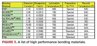
The mention of special preparation for PTH in Figure 5 is in regard to making the substrate active to where it will accept copper plating, as previously discussed. The mention of a standard preparation relates to a standard permanganate, or plasma cycle, typically used for FR-4 materials.
The reference of a re-melt temperature concerns the thermoplastic materials that can reflow or melt in later processes at elevated temperatures. The re-melt could cause the multilayer to delaminate. If a soldering operation would need to be performed on the multilayer, it should be lower than the re-melt temperature or the proper bonding materials selected to endure the soldering operation. The materials that have an “N/A” are thermoset and will not melt or reflow in subsequent processes.
There are no known processes that can desmear PTFE, so when drilling the material, it is of paramount concern to minimize heating and ensure there is no smearing of the substrate. General parameters for drilling PTFE substrates are shown in FIGURE 6.
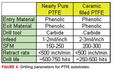
The drill tool should be new and not a re-sharpened tool for the nearly pure PTFE. This will ensure that the cleanest possible cut in the material can be made without smearing. However, a re-sharpened tool can be used for ceramic-filled PTFE substrates. If the circuit board is a hybrid using PTFE and other non-PTFE materials, then the drilling conditions should always be adjusted to the best PTFE drilling conditions. The circuit should be drilled with the PTFE up (toward drill tool entry), if there is only one PTFE outer layer in the PCB stackup.
After the holes have been drilled, the PTFE material will need to be prepared for activation so the copper plating process can achieve a uniform, adherent copper plating in the through-hole. In the case of the nearly pure PTFE substrates, a specialized wet chemistry process is recommended prior to the copper plating process. This process will use sodium naphthalene (or some derivative), which will strip a fluorine atom from the drilled surface in order to make the PTFE substrate wettable and accepting of the copper plating.
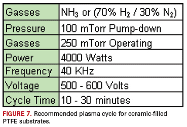
For ceramic-filled PTFE substrates, the same wet process treatment can be applied, but there is a caution that a thorough bake must be done on the panels just prior to the copper plating. The ceramic-filled PTFE substrates can absorb some of the wet processing chemistry. If the PCBs are not baked prior to plating, moisture from the wet process can be sealed into the material behind the electroplated copper in the through-hole. In later processes that involve elevated temperatures, the entrapped chemistry will volatilize and cause delamination of the substrate. A safer process for the ceramic-filled PTFE substrates would be to use a special plasma cycle that can make the substrate wettable so that it will accept metallization. There are two plasma cycles that are commonly used. The parameters for the first plasma cycle are shown in FIGURE 7. The second plasma cycle is similar to the first, except for the type of gas that is used. In this case, the gas mix would be 100% Helium.
Ceramic filled materials have unique demands for the fabricator. Several important fabrication issues regarding ceramic loaded resin systems are: drill tool life is low; drill tools should not be re-sharpened or reused; rough drilled hole wall quality; loose ceramic particles after through-hole wall preparation; prepregs have minimal flow characteristics; and the prepregs are sensitive to low pressure areas during lamination.
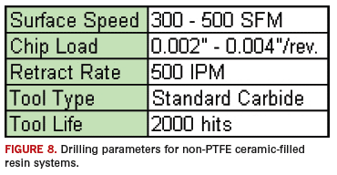
Drilling the ceramic-filled resin systems is more like excavating than drilling. At the through-hole wall, the drill tool will either remove the ceramic particle or let it remain. This makes for a rough drilled hole-wall, which is actually better for plated copper adherence. Drilling the ceramic-loaded materials will damage the drill tool quickly, as well as the flute, and this is why the drill tool should not be reused. The starting drill parameters for this type of material are shown in FIGURE 8.
Minimizing heat to eliminate smear with PTFE is very important, but that is not the case with ceramic-filled resin systems. Of course, it is best to have drilling conditions that yield a good quality through-hole and with minimal smear. These materials can be processed in permanganate or standard FR-4 plasma cycles for desmear. The ceramic particles will not be affected by these processes, so it is necessary to have a high-pressure spray rinse after the desmear process to remove any loose ceramic particles.
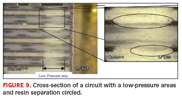
The prepregs that are ceramic-filled resin systems will typically have less flow and will be sensitive to low-pressure areas during lamination. The low-pressure areas are frequently due to the design of the circuit. When there are many copper features aligned in the cross section of the circuit, the areas between these “stacked” copper features will have lower pressure and can cause the resin and ceramic particles to separate and not flow homogenously. The resin separation may have a different CTE than the homogenous prepreg and could have problems with solder or other elevated temperature exposures. To minimize this risk, there are several items to consider. In the lamination process: use a conformal material next to the panels; use the highest pressure possible; at the beginning of the cycle, have a hold for 20 minutes at the temperature where the prepreg will have the lowest viscosity; and ramp up to the cure temperature after the hold. An example of a circuit with low-pressure areas and resin separation is shown in FIGURE 9.
LCP circuit materials offer many unique characteristics for multiple end-user applications. These materials have been available in the industry for a number of years; however, they are not well adopted by traditional PCB fabricators. The reason is due to unique processing requirements and the need for some processes to be extremely well controlled.
Some of the excellent properties of the LCP material are: halogen-free; consistent dk; low TCdk; dk vs. frequency is very good; low dissipation factor; dissipation factor vs. frequency is very good; very high frequency capable; extremely low outgassing; extremely low moisture absorption; no issue with CAF or electromigration; very high MOT (Maximum Operating Temperature) rating; nearly perfect hermetic sealed circuit possible; excellent chemical resistance; inert substrate; and is naturally flame retardant.
An example of a coplanar waveguide tested over a very wide frequency band and with different LCP thickness is shown in FIGURE 10.
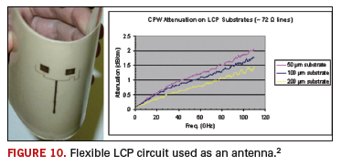
In general, the main issues regarding LCP fabrication are: thin and soft laminates; dimensional stability (scaling) issues like thin flexible circuit materials; special high temperature lamination for LCP multilayers; special PTH preparation; drilling to avoid smear; venting; and border patterns for lamination.
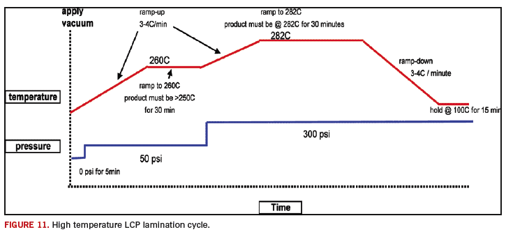
The lamination for a pure LCP multilayer will require a high temperature lamination that is well controlled for temperature and pressure distribution. The lamination materials that will be placed next to the LCP circuit material need to be very conformal. Typically, several sheets of skived Teflon (2 sheets or 3 sheets of 2-mil Teflon) are used. The conforming Teflon sheets offer the benefit of pushing the bond layer of the LCP into the circuit geometry and helping to minimize any detrimental effect due to pressure distribution anomalies.
There will be some small amount of out gassing during the lamination cycle, and since LCP is a very good vapor barrier, having venting holes and good border channels is important. For the inner layer circuit border pattern, a dot pattern should be used to ensure that there are complete venting paths to the outside edge of the circuit panel. These dot patterns should not align layer-to-layer. The venting holes should be drilled through all layers, as many as possible, and are non-PTH holes. Prior to the high temperature lamination, the LCP materials should have had a good acid rinse and a bake at 121°C (250°F) for four hours.
The high temperature lamination cycle uses a dwell at 260° C (500° F) with low pressure and vacuum assist in order to help remove the outgassing prior to raising the pressure and temperature for the fusion bond cycle. This is shown in FIGURE 11.
The drilling operation is also important and has similar concerns as drilling PTFE substrate. The main concern is to minimize the risk of smearing the substrate, which means minimizing the heat generation during the drilling process. Parameters for drilling LCP are shown in FIGURE 12.
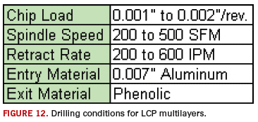
When drilling small holes or high aspect ratio, a peck drilling procedure may be needed. The maximum peck depth should not exceed 0.015 inches. The drill tool should be high-quality carbide and only one new tool should be used.
The drilled hole-wall preparation for PTH can use either a chemical process or a plasma process. The chemical process uses a high concentration of KOH. The plasma process is recommended, and the parameters for this process are shown in FIGURE 13.

There are many PCB applications where combinations of different circuit materials are used. Some applications will have high frequency circuit materials used on the PCB layers that are critical to electrical performance, while the other layers may use FR-4 materials.
A common mixed material PCB uses one layer of a non-PTFE ceramic-filled substrate for Layers 1 and 2, which make up a high frequency microstrip transmission line. The other layers of the PCB are more traditional PCB materials, such as FR-4, and are not electrically critical. With Layer 1 being the signal and Layer 2 the ground plane, the bonding materials below Layer 2 can be FR-4 prepreg. These hybrids can typically be manufactured with good yields, assuming some caution is taken during a few processes. One area of concern would be the unbalance of material types, resulting in a possible warp issue. The most effective procedure to minimize the warp issue of the mixed materials occurs during the lamination cycle, specifically at the end of the cycle and after the prepreg is fully cured. The pressure should be minimized to 50 psi and held for 30 minutes. This low-pressure cycle is held while still at the cure temperature.
Another common mixed material PCB combines a ceramic-filled PTFE substrate and FR-4. The ceramic-filled PTFE is a closer match to the FR-4 thermal/mechanical properties and will result in a simpler PCB process. The PTFE substrate typically does not warp because it is very soft compared to the FR-4. During the lamination cycle, the FR-4 substrates will expand/shrink due to the temperature excursions, and the PTFE will be so soft that it will follow the FR-4 movement. The drilling must be tailored to be optimal for the PTFE, and the preparation for PTH will have several stages. The first stage is to desmear and treat the FR-4 material as necessary for the PTH preparation. The next stage will be to treat the PTFE for the PTH process. If a wet PTH preparation process is used for either the FR-4 or the ceramic-filled PTFE, then a bake at 121°C (250°F) for 1 hour to 2 hours is necessary just prior to the copper plating process.
A special rigid-flex construction is a more exotic hybrid combination that has the potential to be extremely good for high frequency applications and has mechanical flexibility. This circuit would use the LCP materials for the flexible portion and the non-PTFE ceramic substrates for the rigid portion. This combination would have several advantages. The transition from the rigid board areas to the flexible areas will not have connectors, and the connection is built into the circuit. The lack of connectors means the cost for the connectors, assembly and reliability issues of connectors goes away. Also, if the design accounts for the transition from the rigid material to the flexible materials correctly, there can be no impedance difference, resulting in a clean signal transition. For this type of circuit, the drill parameters will need to use the LCP parameters. The plated through-hole preparation will be several stages, as previously described. The last stage of the preparation process will be for the LCP materials.
While PTFE substrates can be more difficult to fabricate, they do deliver superior performance. The best material for electrical performance is the nearly pure PTFE substrates. These types of materials have been used for the most demanding electrical applications and have very specific fabrication guidelines. Adding ceramic filler to the PTFE will lower the CTE, which is good for multilayer circuits and PTH reliability. This addition also makes the material friendlier to PCB fabrication; however, it slightly degrades the electrical performance.
The non-PTFE materials are typically the most friendly to the PCB fabrication process and can have good electrical properties. There are many types of prepreg that can be used with this type of material, and most of them have very different processing guidelines. Lastly, the LCP materials offer a multitude of benefits to many applications. However, the PCB fabrication process requires special equipment and must be well controlled.
In summary, each type of high frequency material has its own unique circuit fabrication concerns. Sometimes there are interactions between the high frequency circuit materials and the PCB fabrication process that can affect the circuit performance for the end user. That is why it is critical for PCB fabricators to understand the specific processing concerns related to these materials. Understanding the materials’ unique processing requirements will help the PCB fabricator achieve good manufacturing yields along with high quality and increased reliably in the finished circuit board. PCD&F
REFERENCES
1. John Coonrod, “Bending and Forming High Frequency Printed Circuits”, IPC Printed Circuits Expo, APEX and the Designers Summit, 2007.
2. Thompson, Kirby, Papapolymerou, Tentzeris, “W-Band Characterization of Finite Ground Coplanar Transmission Line on Liquid Crystal (LCP) Substrates,” IEEE Polytronic Conference 2003.
John Coonrod is a market development engineer at Rogers Corporation; This email address is being protected from spambots. You need JavaScript enabled to view it..


