IC Package to PCB Co-Design
Advances in IC packages provide designers with pin assignment control that reduces routing time, improves signal integrity and reduces layer count.
Many interesting assembly methods and packaging techniques have been explored in the past to overcome the challenges of trying to make more features fit in less space. One can say the printed circuit board itself was a revolutionary technology that enabled low-cost mass production of electronic equipment, well before semiconductors were put into widespread use. However, aside from the complexities of their production, PCBs presented a new set of challenges for engineers and manufacturers to overcome. Design in the consumer space, for example, was a constant tradeoff between size, look, function, user interface (psychology), power, reliability and yield. New interconnect technology required new packaging for components, which in turn required new assembly machinery and practices. Vacuum tubes for small appliances went to pig-tails rather than sockets, but their pin configuration was still largely dictated by the physical design of the plate, grid(s) and cathode within the envelope. New machines had to be created for the preparation and preforming of component leads, then along came the transistor. So the drive continues toward making things smaller, faster, better.
At each step of the way, the configuration of device pins has largely been dictated by the internal physical structure of the device in question. Even today, we still use many devices that have a pinout that, to the PCB designer, is far from sensible. When you consider the cost and complexity of the actual chip design and constraints of power consumption and timing, this is hardly surprising.
Another evolutionary step in the electronics industry was the development of MSI, LSI and then VLSI (Medium/Large/Very Large Scale Integration) COTS (Common-Of-The-Shelf) components. Most notorious among these are the 7400 standard logic series and their pin-compatible descendants, as well as various transistor arrays and de facto standard analog parts like the 741 op-amp or the LM7805 regulator. Throughout the 1980s and 1990s, I used many of these components in designs, and I always lamented over the seemingly ridiculous pinouts of many useful devices that made my life difficult as a budding design engineer.
Without Co-Design
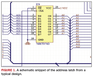
A case in point: Most of the design projects I was involved with involved microcontrollers such as the MCS-48 and MCS-51 families. These devices have since spawned countless derivatives with different packages, but at the time, they were constrained to a 40-pin DIP. To fit all the address and data lines required for the memory interface, the manufacturers had to multiplex the device pins. I had to use a separate 8-bit latch device to hold the low address byte while the data were being transferred across the bus. There’s a handy pair of devices in the 74xx series, the ‘373 (octal transparent latch) and ‘374 (octal D-type flip-flop) respectively, that took care of the address de-multiplexing. A schematic snippet of the address latch from a typical design is shown in FIGURE 1.
The ‘373/4 was a classic case of a horrible pinout. The schematic looks great, but when you bring it over to the PCB, you have a lot of crossovers and a tough time routing it as seen in FIGURE 2. A common trick to mitigate this was to change the order of the flip-flops on the schematic by manual pin swapping, creating a library of alternatives. In the 1980s and 1990s, PCB design tools were very limited, and none had pin-swapping automation. This problem often resulted in confusion or error, and in the worst case, the program memory was not read in the correct sequence, resulting in a re-spin. So as the 74xx series evolved, easier devices were released, largely owing to silicon processes allowing an extra layer of die connections. Then the pinout improved to favor the PCB.
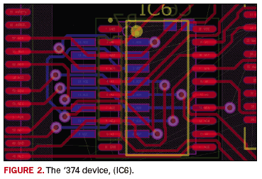
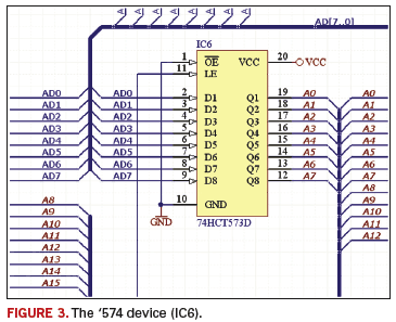
FIGURE 3 illustrates the newer ‘574 device (IC6). Note the pin numbering sequence as compared to Figure 1.
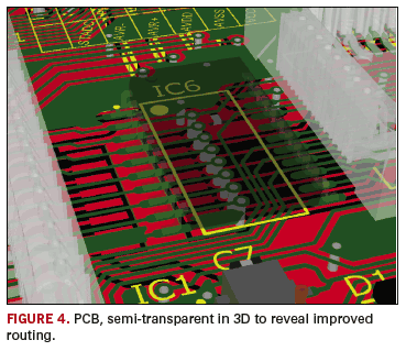
Naturally, it made for a much faster job routing the PCB and resulted in a neater design with lower via count required. Hence, overall product cost was reduced. The updated PCB is shown in FIGURE 4. IC6 is shown semi-transparent in 3D to reveal improved routing.
These innovations – including surface mount – significantly improved designs where component density was paramount. But to obtain the density required for certain applications, it was necessary to eliminate the package altogether. Making use of chip-on-board and wire bonding presented a whole new challenge. Other hybrid technologies, such as thick film printed components, were also a challenge. Higher levels of integration in silicon proved to make these methods short-lived with hybrid circuit assemblies being popular through the mid 1980s, yet they are making a comeback in medical and aerospace today.
Co-Design Today
ECAD tools need to be flexible in order to cater to such specialized applications. Most tools allow customization via scripting to add functionality that is peculiar to their product or industry, but tools that have a more abstract and flexible approach at viewing and editing design data make it easier and can remove any need for customization.
Development of denser packaging throughout the 1990s up until now has improved the situation but it’s a double-edged sword:
We do not deal with multiplexed buses as often, but instead we have numerous extra connections coming out of the center of the package (i.e., BGAs).
The more complex packaging requires extra layers from the PCB for fan-out, finer tolerances for manufacturing, extended layout and routing times and challenges with yield.
These factors result in higher product costs to the consumer. To mitigate current and future tradeoff problems, there are a few approaches that can be taken.
If you have the luxury of developing the PCB in concert with the ASIC package designer, or better still, you perform both functions, then you can work within that model and improve the package to facilitate better PCB design. This puts the onus back on the ASIC designer, and in this case, it is worth looking at alternative methods for improving connectivity at the silicon level. There is also the weighting of costs and time involved in tradeoffs, such as silicon-thru-via vs. multi-chip-module vs. flip-chip or wire bonding techniques. It is important to note that in essence, both the PCB designer and the ASIC designer work with placement, routing and layers of metal. So the tradeoffs can indeed be shared or moved from one domain to the other. In any case, both must be willing to work in a closed loop and to collaborate and share ideas and design data. Therefore, there needs to be mechanisms within the design tools that easily facilitate such transfer (e.g., CSV/Spreadsheet style global editing, smart pasting of design data and collaboration via version controlled design repositories).
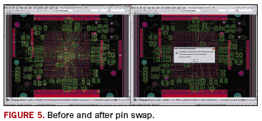
Today’s design tools have pin-swapping capabilities that go a long way toward solving the problem. These allow the designer to automatically swap gates within a package or pins within each gate where appropriate. This capability spans from simple components, such as decoupling caps and resistor packs, to the most complex BGAs. The idea is to pre-configure components to allow the tool to know which pins are equivalent based on design rules and constraints, then interactively, or in an automated pass, allow it to reduce the routing lengths and crossovers within the rat’s nest. FIGURE 5 shows before and after shots of this process.
Providing a pin-swapping capability is only half the story. In most cases, the package of the device in question still has a fixed-function pinout. For example, even tricks that used to apply with memory devices that treated address and data signals as a homogenous group (allowing them to be arbitrarily swapped) are no longer feasible with current memory technologies, due to the fact that address buses are used to access internal configuration registers, requiring a fixed bit-order. Aside from that, there are also banking and interlacing issues. Then there is the other end of the bus, typically a microprocessor of some sort. It is increasingly common for it to be a high pin count BGA. Even with modern packages, in which the core power and grounds are well positioned toward the middle and the IOs around the edges, the tendency of chip manufacturers is to have most GPIOs share a fixed-function peripheral port that you cannot change. Even if the IOs you need are at the edge and easily accessible, you still often need to route around the entire device to get the connections going in the directions you need.
State of the Art
I am a firm believer in disruptive technology – every now and then something comes along which, at first, may under perform the sustaining technology it competes with, yet offers an irresistible benefit to early adopters who have a need for its flexibility or inherent features. Eventually, with due seasoning, it yields an alternative solution that has no drawbacks. FPGAs are one such technology. Look at the overall growth of FPGA manufacturers and the undeniable performance improvements FPGAs now offer in many applications. Link this to increases in FPGA design starts vs. traditional ASIC design starts, and it is clear that it’s a technology with the power to change how things are done.
So what does this have to do with package-PCB co-design, you ask. Apparently, a lot. Of course, one of the technology’s strong points is the fact that the GPIOs are exactly that – general purpose IOs. An FPGA IO pin (and more importantly, the buffer that connects to the pin within the device) is typically capable of supporting in excess of 15 different signaling standards (LVTTL, CMOS, STL, LVDS, HSTL, LVPECL). In addition, there are usually no fixed-function (meaning fixed in hard silicon) peripheral cores directly linked to a given IO bond pad. Instead, the IOs sit alongside vast multiplexors and on-die routing resources that allow the FPGA designer to specify which pins to use for their given purpose. Bear in mind, a trade-off exists between fitting the design on the target FPGA and obtaining timing closure versus allowing the PCB layout to entirely govern the pin assignments. But to a great extent, the PCB designer can have a say in how the pin assignments are made, reducing PCB routing time, improving PCB signal integrity and potentially reducing the number of required layers.
What this means is that with FPGAs, we have the freedom to swap pins and IO banks to improve the layout, but the design tool is then used to push the new net connections back to the schematic and forward to the FPGA constraints file – all through a salubrious ECO process.
Conclusion
Here is where the future looks very bright. Because this technology exists today in CPLDs and FPGAs, many of the patents held regarding configurable IOs are now nearing the end of life. Between the next three to five years, we are likely to see many additional chip vendors augmenting their devices with programmable IO pin capabilities and programmable routing resources similar to what is available today in FPGAs. Imagine an 8051 derivative with a JTAG debug port that also allows the user to completely define their own custom pinout that suits their product. Imagine an ARM microcontroller that has reconfigurable IO with crossbar switches and user-defined SERDES capability, where YOU can decide which pins will be clocks and which will be I2C IOs. As ECAD tool and silicon IO technology advances, we can expect to attain the optimal pinout for every design, without sacrificing product performance or the designer’s time. PCD&F
Benjamin Jordan is a field applications engineer with Altium Inc; This email address is being protected from spambots. You need JavaScript enabled to view it..


