Designing with High Frequency Materials

Understanding the primary and secondary performance requirements in a high frequency application can help designers determine the most suitable materials to use.
Specialty high frequency circuit materials have been used in the PCB industry for decades. There are several attributes of these materials that are very unique when compared to the more traditional FR-4 materials. Understanding these attributes can help the OEM, designer and fabricator optimize the application and maximize the potential for improved electrical performance on the products that are being developed. There are additional, non-electrical advantages to these materials as well. In order to realize the full potential that these materials have to offer, it is important to understand the specific application and design constraints that need to be addressed.
Most high frequency applications will place multiple demands on the PCB material, and some of the requirements may be contradictory. For a specific application, one requirement is often paramount, while the others are secondary. Understanding the primary design considerations and specific requirements for the high frequency materials will allow the designer to choose the optimum material for the application. Several example applications will demonstrate how the various attributes of the product need to be considered in order to determine the optimum material to be used.
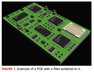
The first application example is a small filter circuit using high frequency materials that will be soldered to a larger FR-4 circuit board, as shown in FIGURE 1. The completed assembly will be housed inside a sealed enclosure and will operate in an outdoor environment that varies greatly by the seasons. Added to this is the specific heat generated by the equipment. Temperatures inside the enclosure could vary from –25 °C to +70° C.

Filter circuits typically need a material with very consistent dielectric constant (Dk). This means consistent Dk within a sheet of circuit material, as well as from lot-to-lot. This is required so the filters being attached to the FR-4 circuits will have the same performance, and minimal part-by-part tuning will be necessary. This filter will be a double-sided plated through-hole (PTH) circuit, with the ground plane on the bottom and the signal plane on the top, coupled to the FR-4 circuit board using a microstrip edge coupler. As previously mentioned, most high frequency applications have more than one demand on these circuit materials. In this case, the consistent Dk is paramount, but there are other demands that also need to be considered as secondary.
All circuit materials have some amount of growth or shrinkage due to heating or cooling of the material, due to the coefficient of thermal expansion (CTE). In this case, the CTE may not appear to be important, but it can be critical. Once the filter is soldered onto the FR-4 circuit board, the solder joints become a rigid bridge between the FR-4 circuit and the high frequency filter. When the unit experiences a change from 0° C to +30° C (as an example), the FR-4 and the filter circuit will expand. If the CTE is significantly different between the FR-4 and the filter material, stresses can develop at the solder joints that connect the circuit board to the filter, and this may become an issue over time. In most cases, one excursion from 0° C to +30° C is not a problem, but with repeated cycling, the solder joints become stressed and the electrical connection can be compromised.
Another critical issue is that of the material’s temperature coefficient of dielectric constant (TC Dk). Each type of circuit material has a property where the Dk value can change with a temperature change, and that is the temperature coefficient of dielectric constant. With certain circuit materials, the Dk may appear to be good and consistent when tested at room temperature; however, as the temperature changes, the Dk can change and cause the filter to perform significantly different than as designed.
An additional consideration is the assembly operation, where the filter is soldered to the FR-4 circuit board. Since the filter has plated through-hole vias, the z-axis (thickness) CTE can become a concern during the soldering operation. Depending on the design of the filter and the FR-4 circuit board, the dwell time during soldering may need to be adjusted, particularly if thick materials and heavy copper are used. If the circuit material has a higher z-axis CTE than the filter material, an extended dwell at elevated temperatures can cause damage to the plated through-hole vias and degrade the electrical connection from the signal plane to the ground plane.
Lastly, if the filter is intended to operate over a wide range of frequencies, it is important to understand that most circuit materials will have different Dk values at different frequencies. It should also be considered that some materials are more stable than others.
In summary for this application example, this filter circuit should use a material that has a tight tolerance for Dk, a CTE that is closely matched to FR4 in the x-y plane, a low TC Dk, a low z-axis CTE and a stable Dk vs. frequency curve. There are many high frequency circuit materials to choose from but finding the right circuit material, which fills all of these requirements, will reduce the available choices. A comparison between the properties of a standard FR-4 circuit material and the material under consideration for the best choice is highly recommended. For this example, the typical values regarding the properties of interest for a standard FR-4 material are shown in FIGURE 2. The user will need to determine the fitness for use of the selected materials by conducting appropriate short-term and long-term reliability testing as dictated by the needs of the application.

Additionally, if it were critical to reduce the physical size of the filter, a different circuit material with a higher dielectric constant may have been the right choice. A material with a higher dielectric constant will allow the circuit to be reduced in size while still performing the same function. The high frequency circuit material used for this filter application may not actually be used at a relatively high frequency. The material may have been selected due to its tight Dk values and the other properties mentioned. Another item where most high frequency materials have an advantage over more traditional FR-4 circuit materials is minimal moisture absorption. Having low moisture absorption is important for several reasons, including the fact that in high frequency applications where consistent Dk is critical, moisture absorption can be a problem. Water has a Dk value of about 70, and even a small amount of moisture absorbed into a high frequency circuit or a controlled impedance circuit can change the electrical performance.
The second application example is a microstrip circuit that will need to be formed to a specific shape around a mandrel that has a 0.5-inch diameter. The electrical concerns are primarily low insertion losses (< 0.05 dB/in), tightly controlled impedance (50 ohms +/- 5%) and operating considerations at 900 MHz. Typically, an application operating at 900 MHz is not considered high frequency and more traditional FR-4 materials could normally be used. There are however, other electrical concerns that drive material selection to a high frequency grade material in this example.
The need for tightly controlled impedance translates to a substrate that must have tightly controlled thickness and Dk values. Traditional FR-4 materials will not control these attributes nearly as well as high frequency circuit materials. Of course, the etching of the conductor width will need to be tightly controlled at the circuit fabricator to meet the controlled impedance targets.
Overall, the concern of low insertion loss can be rather complicated. There are many issues that can affect this circuit property such as: connectors, signal launch design, plating finish on the copper conductors, dissipation factor of the substrate, copper roughness, circuit geometry and some assembly processes. When choosing the material that will give the best advantage for insertion loss, a material with low dissipation factor, smooth copper and low moisture absorption would be optimum. Also, the circuit design should use a relatively thick substrate.
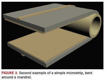
In this case, there are additional concerns with the mechanical challenge of forming a circuit around a mandrel (FIGURE 3). Typically, a thinner substrate with no glass reinforcement will be better for forming the circuit and will generate less strain on the copper layers. Also, the copper type should be rolled wrought or rolled annealed copper, which has a grain structure that is optimum for elongation in the x-y plane.1

Another consideration could be the type of plating finish applied to the copper conductors of the microstrip. If ENIG (electroless nickel / immersion gold) is used, then the nickel is brittle and can be problematic for bending. Also, the ENIG process will typically deposit a thickness of approximately 100 microinches to 200 microinches of nickel and about 5 microinches of gold. With the operating frequency at 900 MHz, the skin effects will force the signal to use about 87 microinches of conductor. That means the signal energy will predominately use the nickel layer, and nickel will cause an increase in conductor losses and ultimately insertion losses. This is due to the fact that nickel is less conductive than copper and has a permeability value that is much greater than copper. The permeability value will adversely affect the magnetic fields of the propagating waves.
For this application, designers should choose a high frequency material that has a tight control of the Dk and thickness tolerances, low dissipation factor, smooth copper, non-glass reinforcement, low moisture absorption and a non-nickel/gold finish. To determine the optimum thickness, there will need to be a trade-off between mechanical and electrical properties. For a one-time bend, there is a rule of thumb that states the strain on the copper should be approximately 2% or less. FIGURE 4 shows a comparative table of different materials and thicknesses in regards to the mechanical stress values and insertion losses.

In Figure 4, it can be seen from the first model to the second that the thickness of the substrate decreases. The decrease in thickness improved the mechanical stress significantly. A decrease in the substrate thickness will force a decrease of the conductor width in order to maintain 50 ohms. The decreased conductor width will increase the conductor loss, and ultimately, the insertion loss.
When going from the second to the third model, a different material was selected that had a lower dielectric constant and lower dissipation factor while still maintaining the same substrate thickness. The lower dielectric constant dictates an increase in conductor width to maintain 50 ohms. The increase in conductor width lowers conductor losses, and the decrease in dissipation factor lowers dielectric losses. With lower conductor and dielectric losses, insertion loss also decreases.
It can be seen that the stress number is a little higher than would be desired, but when looking at other models, this appears to be the best-case scenario. In reality, this may be good enough for the actual application. If in practice this model does not result in good, repeatable bends, the mandrel may need to be increased in size to lower the stress.
When using high frequency materials in a PCB design, it is important to understand the primary performance requirements of the final product so that the best material can be selected for use. Most high frequency materials are used in specific applications where low electrical loss and uniform electrical performance across frequencies is needed. In addition, low moisture adsorption and excellent chemical resistance are salient properties of many high frequency materials and can be advantageous in specific environmental applications. PCD&F
Ed. Note: In Part 2 of this series on high frequency materials, fabrication processes will be investigated.
REFERENCE
1. John Coonrod, “Bending and Forming High Frequency Printed Circuits”, IPC Printed Circuits Expo, APEX and the Designers Summit, 2007.
John Coonrod is a market development engineer with Rogers Corporation; This email address is being protected from spambots. You need JavaScript enabled to view it..


